Machine vision targets semiconductor inspection

Combining sophisticated lighting, multiple cameras, and custom hardware allows semiconductor wafers to be rapidly inspected.
By Andrew Wilson, Editor
Wafer bumping is a fast-growing method of packaging silicon for high-density and high-frequency applications. The bumping process is constantly being improved and cost is decreasing, making these interconnect methods more popular. To enable this technology, semiconductor-inspection systems are now incorporating sophisticated machine-vision lighting, camera systems, and high-speed image-processing systems to ensure the integrity of the devices.
Wafer bump inspection and flip-chip substrate bump inspection are performed on similar geometries and are essentially opposites of the same interconnect package once the wafer is diced. The main difference in inspecting wafer bump and flip-chip substrates is that wafer bump inspection dictates higher magnification optics.
“Solder balls used on many ball-grid-array (BGA) devices and flip-chip substrates are designed to be the same height, so when BGA devices are placed on printed-circuit boards (PCBs) all the balls make an electrical contact with the pads,” says Alain Gagnon, R&D director at Boreal Vision Solutions. “But even if all the balls are the same height, warping of the component or PCB can prevent them from making a good electrical connection. In the worst case, the contact may be very weak and will break and the component will repeatedly expand and shrink during the operation.”
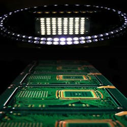
To overcome these inspection challenges, Aceris 3D Inspection has developed an automated visual inspection system that enables manufacturers to identify dropped, tilted, or chipped components (see Fig. 1). Using an LED ringlight, structured laser-light illumination system, custom and off-the shelf CCD and CMOS cameras, and custom image-processing hardware, the AI-808WB wafer-inspection system provides an effective resolution of 0.08 µm and can inspect between 20 and 60 wafers per hour. Typical bump functions performed by the system include height, diameter, and coplanarity measurement and detection of misplaced and/or missing bumps.
Data acquisition
For high-speed inspection of solder bumps, Aceris 3D Inspection systems have a single sensor head that incorporates three different light sources, two high-resolution cameras, and a structured-light source. “Laser triangulation sensors have particular advantages in speed, since the acquisition of the surface geometry is achieved in a continuous motion, while other 3-D sensors must acquire a multitude of images of a relatively small wafer area standing still and then moving to the next location,” says Gagnon. “Moreover, the motion-control systems need to accelerate and decelerate rapidly, which mandates heavier and more expensive solutions.”
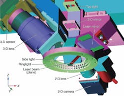
To perform visible and structured-light measurement required incorporating both technologies into a sophisticated sensor head. Using a visible LED light source, the system had to image both the background of the wafer substrate and the solder bump itself. To do this, Boreal Vision Solutions incorporated a cloudy-day illuminator (CDI) like system based on two 8 × 8 panels of white LED lights placed at 45˚ within an LED ringlight (see Fig. 2). “While the 45˚ illumination system captures images of the background substrate of the wafer,” says Gagnon, “the white LED ringlight provides images of the solder bumps themselves.”
Because the ringlight can be used in darkfield, brightfield, and side mode, it is especially useful in semiconductor inspection applications to detect bump diameter, area, and position, and for large-defect detection. “While brightfield illumination can detect the changes in light intensity caused by pinholes and coating voids, darkfield lighting is useful for detecting scratches and streaks on the substrate. CDI mode is optimal for inspecting specular surfaces where any lighting reflections will cause defects to appear or the vision system to see defects where none exist.
To visibly image the substrate and solder bumps as the sensor head is moved across the machine gantry, an Adimec-1000m, 1004 × 1004 pixel 50 frames/s, CCD camera with a Camera Link interface is used. With a transfer rate of over 80 Mpixels per second, this camera is interfaced to a host PC using an off-the-shelf frame grabber.
Structured light
When using mirrors, beamsplitters, and filters to separate the visible light used for the 2-D imaging from the laser light used for triangulation, both the optical and laser modules have the same optical axis and view at the same area of the substrate through the ringlight. This allows for simultaneous acquisition and processing of both visible and structured-light data and avoids the use of separate scans.
To achieve this multiple scanning mode, the geometry of the sensor has a custom 30-mm structured laser source projected at 45° to the wafer surface. As the sensor head moves across the wafer, the reflected laser light is captured by a high-speed CMOS imager.
Aceris custom-built a camera head and a Camera Link interface board that is incorporated into the sensor to capture data at this rate. Captured laser light from the sensor is transferred to a custom-built PCIX-interface board using a Medium Camera Link interface. To process such a high data rate, the custom frame grabber/processor must convert laser line images into x, z surface profiles at rate of more than 25M coordinate points per second and transfer the data for processing on dual-core processor running Windows XP.
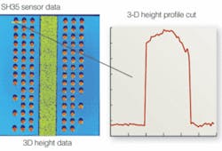
As the laser light is reflected from the surface of the BGA, the CMOS camera detects the bright points along an imaging ray, in a sequential 2352 × 1 fashion. The frame-grabber board computes the 3-D surface points (see Fig. 3). After the surface profiles are computed, they are displayed on the host PC monitor.
Surface profiles
“Because of the large number of profile points (2350), a relatively wide swath (or profile width) of more than 8 mm can be achieved. “This results in 3.5-µm resolution across the x-axis, 0.08 µm in depth (z), and a scan direction (y) that is programmable in 0.5-µm increments,” says Gagnon. “A programmable step size is another advantage of using laser triangulation, since the resolution in the scan direction (y) can be adjusted for optimal speed, required precision, and given bump size and geometry.
“Although the structured laser source provides a view of the top of the BGA, detecting the edges is more difficult to perform with these methods,” says Gagnon. To do so requires an analysis of the optical image data that is captured by the Adimec CCD camera. When combined, the complete system provides a defect map that is superimposed on the final image so that the final system is capable of 10,000 laser profiles per second and a scanning speed of 35 mm/s. This high acquisition speed allows for an inspection rate of more than 40 wafers per hour for 8-in. wafers.
Isolated from the external vibration by antivibration pads on the cabinet level and on the gantry level, the scanning system moves wafers held by a vacuum on a wafer chuck. Because the wafer chuck is fixed to the gantry, there is no unintended relative motion between the sensor head and the wafer being inspected.

Features, advantages, benefits
“Aceris 3D Inspection designs, produces, and sells inspection systems using Boreal’s illumination component integrated into its combined 2-D/3-D sensor for the inspection of solder paste on PCBs, wafers, and flip-chip substrates,” says Bojko Vodanovic, president of Aceris. “The new advanced 3-D camera can capture 10,000 images/s, which is equal to 100 mm/s with 10-µm distance between separate 3-D snapshots.
“When even higher accuracy is required,” Vodanovic says, “Aceris 3D can offer a laser sensor module with 0.08-µm resolution. By combining all these components into a single unit, the system is simpler to calibrate and more reliable. This also simplifies integration of the sensor into third-party equipment, such as solder-paste printers.”