SOLAR ENERGY: Smart camera inspects solar wafer codes
Two types of crystalline silicon are used in the production of solar cells. In the first type, monocrystalline silicon solar cells are produced by slicing wafers from a single crystal boule. In the second, multicrystalline silicon is first cast into a block, which is cut into bars and then wafers. In the manufacture of these multicrystalline wafers, solar cell manufacturers need to closely monitor the production process.
Because of this, each wafer must include information about the bar it is made from and the position within the bar where it has been cut out. Since this information cannot be inscribed on the surface of the wafer, it must be placed on the edge.
“Before multicrystalline bars are cut into wafers,” says Eckard Eikelmann, president of FiberVision (Würselen, Germany; www.fibervision.de), “laser marking is used to encode the manufacturer’s data on the side of each bar.” To accomplish this, the 600 × 156 × 156-mm3 bars are marked along their 600-mm horizontal axis with a laser. Inscribing multiple laser lines at different spacing along this edge before the bars are cut results in a barcode-like pattern on each wafer. This information codes the identification of the bar.
“In a similar manner,” says Eikelmann, “laser marking the side of each bar with a sawtooth pattern will indicate the position of each wafer, once cut, within the bar.” Both of these codes containing the manufacturing data and the position of the wafer in the bar are inscribed to appear at two distinct positions within 80 mm on the side of the wafer. Once cut into about 200-µm-thick wafers, this information must then be read as the wafers move at 220 mm/s through the production process.
To accomplish this, FiberVision first developed a smart 5-Mpixel camera based on a VCSBC4012 nano single-board camera from Vision Components (Ettlingen, Germany; www.vision-components.com). Using a 2592 × 1944-pixel CMOS imager from Aptina (San Jose, CA, USA; www.aptina.com), an embedded 400-MHz TMS320C64 DSP from Texas Instruments (Dallas, TX, USA; www.ti.com), and 64 Mbytes of on-board memory, the Nanosmart-PoE power over Ethernet camera runs at 11.6 frames/s.
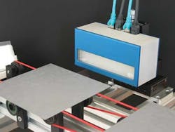
Although FiberVision offers this camera as an OEM component, it was necessary to adapt the camera for barcode wafer inspection. “Because the field of view required is 156 mm,” says Eikelmann, “it was necessary to develop a wafer scanner that uses two of these cameras embedded into a single housing with LED lighting” (see figure).
By using two 12-mm f/2.8 lenses on each camera, two images of each individual barcode are taken as the wafer passes across the image sensor’s field of view. “However,” says Eikelmann, “as the Aptina CMOS imager used in each camera features a rolling shutter, the LEDs must be properly triggered as the wafer moves along the production line.” As each camera features eight digital 24-V I/O lines and a 24-VDC power supply over an RJ-48 connector, these embedded LEDs could be triggered directly from the camera.
After images are captured, they are processed by embedded barcode software running on each of the scanner’s DSP processors. The code, which was especially designed for this application, allows the scanner to inspect up to 3600 wafers/hour. After each barcode is read, the data are then transmitted over Ethernet to a host PC where it can be stored and further analyzed using database software. To allow the operator to visualize captured images, the Ethernet interface is also used to transmit images captured by the scanner to the host at rates of 1–2 images/s.
According to Eikelmann, FiberVision developed the barcode reader as an OEM solution for Hennecke Systems (Zülpich, Germany), which is a member of Meyer Burger Technology Group (Thun, Switzerland; www.meyerburger.ch). Hennecke Systems equips its solar wafer handling, automation, and measurement systems with this reader.
More Vision Systems Issue Articles

