Solar Smarts
Andrew Wilson, Editor
Today’s in-line solar wafer inspection systems must provide a number of measurements to ensure the integrity of the final product. These include detection of barcodes that may be placed along the edges of the wafer; determining the bow of each individual wafer; inspecting the surface of the wafer for saw marks, chipping, and edge defects; and flagging wafers for any micro-cracks that may be present.
Because of the expected growth of this market, a number of OEM suppliers and system integrators are developing products and subsystems specifically to address these tasks. At VISION 2009, held in November in Stuttgart, FiberVision (Würselen, Germany; www.fibervision.de) described the development of a DSP-based camera subsystem that uses two 2592 × 1944-pixel CMOS imagers from Aptina (San Jose, CA, USA; www.aptina.com) to read barcodes on the sides of solar wafers at speeds up to 3600 wafers per hour (see “Smart camera inspects solar wafer codes,” Vision Systems Design, January 2010).
Then, Doug Wilson, co-founder of PVI Systems (Niantic, CT, USA; www.pvisys.com) described in a Vision Systems Design webcast how his company had developed a machine-vision system using software from National Instruments (Austin, TX, USA; www.ni.com) to measure busbar, finger, and paste smear defects on the surface of solar wafers (see "Machine Vision for Solar Cell Inspection").
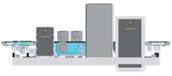
Now, Tordivel Solar (Oslo, Norway; www.tordivelsolar.com) has built on the experience gained in the development of a solar-wafer bow inspection system with a system specifically targeted for surface measurement analysis. The surface instrument is a part of Tordivel Solar WIS – Wafer Inspection System that includes a complete electrical and optical characterization and sorting into 13 boxes or classes. Like the system developed by PVI Systems, Tordivel’s surface inspection equipment uses linescan cameras to image the 156 × 156-mm wafers as they pass along a conveyor and through the vision workstation (see Fig. 1).

| FIGURE 1. Tordivel Solar has developed a solar wafer surface-measurement analysis system that uses linescan cameras to image the 156 × 156-mm wafers as they pass along a conveyor and through the vision workstation. |
Wafer inspection and analysis
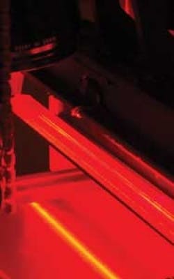
To detect chipping and edge defects, it is necessary to inspect both sides of the solar wafer. The Tordivel Solar Surface Instrument uses two 4k × 1 linescan Camera Link cameras from Basler Vision Technologies (Ahrensburg, Germany; www.baslerweb.com), which are placed above and below to image singulated wafers as they move between conveyor mechanisms. Image data from both these cameras are then transferred to a host PC using a Solios frame grabber from Matrox (Dorval, QC, Canada; www.matrox.com). To ensure wafer defects are properly imaged, two custom 200-mm, linear red LED lights provide angled illumination of both sides of the wafer.
“Because each wafer scan results in two 32-Mbyte images that must be processed rapidly,” say Thor Vollset, president of Tordivel, “edge fault and chipping analysis of both sides of the wafer are partitioned using an Intel i7 hyper-threaded quad core PC, allowing both images to be processed in less than 900 ms.”
To perform the edge fault and chipping analysis, Tordivel Solar uses the Scorpion Vision software package developed by its sister company, Tordivel (Oslo, Norway; www.scorpionvision.com). This software includes a number of image-processing algorithms such as region of interest (ROI) specification, blob analysis, and edge detection tools to determine the integrity of the solar wafer.
“After images of the wafer are digitized, it is necessary to determine if any large breakages have occurred,” says Vollset. Because the area of the solar wafer is known, blob analysis is first used to analyze the area of the wafer being inspected. If this area falls below a certain threshold, then it is automatically rejected since the wafer may be severely broken; no further image processing takes place.
“After wafers pass this first inspection, a more accurate measurement of the edges of the wafer must be made,” he adds. This is complex because images of the wafers are captured while moving; this motion must be taken into account when determining whether edge defects are present or whether they appear to be present due to motion. First, the Scorpion Vision software estimates the correct shape of the wafer and the edges determined by thresholding wafer images (see Fig. 2).
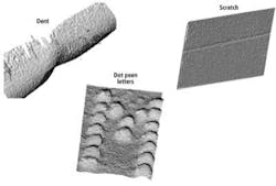
To dynamically locate all of the edge points of the wafer, Vollset and his colleagues used polygonal mapping to approximate any curved edge that may be present. Then by measuring the change rate of the pixel distances along the edge of the wafer, edge defects can be determined (see Fig. 3).
“If this rate of change is slow, it may be caused by the motion of the wafer as it moved across the linescan camera. If the rate of change is of high frequency, it may indicate the presence of a crack in the wafer,” Vollset says. Since the tolerances of a perfect wafer are known beforehand, these can be compared with any deviation along multiple points of the captured image to determine the size of each defect.
“Such measurements are more difficult to perform in wafer corners, however,” he notes, “since these areas are more susceptible to defects and fitting such an area with a known wafer model is more complex.” To determine whether defects are present, ROIs are first generated around edge areas and sub-pixel interpolation used to resample these areas, which are then measured to 0.0032 mm2 using blob analysis (see Fig. 4).

FIGURE 4. Since measurements are more difficult to perform in wafer corners, ROIs are first generated around edge areas and sub-pixel interpolation used to resample these areas. Defects are then measured using blob analysis.
Once determined, defects can be detected in a similar manner as before. While the present system is used to inspect for edge defects and cracks, Tordivel Solar is developing a more sophisticated system that will be used for wafer surface analysis of features such as busbars, fingers, and smears.
“In the same vision inspection enclosure,” says Vollset, “an optional two additional linescan cameras—this time Basler’s GigE-based Runner series—will transfer images to the same industrial PC to perform contamination inspection tasks. With the increasing focus on quality we believe that the largest percentage of wafer returns is at the moment due to contaminated wafers.” The complete Tordivel Solar wafer inspection system is capable of detecting most of the features required by today’s solar inspection industry and is claimed to have an investment payback of less than six months.