Color Camera Cubes
Andrew Wilson, Editor
To add greater functionality to their offerings, designers of cell phones and computers are adding imaging capability in the form of embedded color cameras. Driven by this demand, camera module manufacturers are developing products known as wafer-level cameras (WLCs) to reduce the cost and size of these electronic devices and the related manufacturing expenses.
Although the main market for camera modules is consumer products, the devices will also find use in medical, aerospace, surveillance, and mobile robotics applications where size and advanced capability are of prime importance.
In the past, miniature color cameras were developed by assembling individual lenses, filters, sensors, and readout electronics onto flex circuits. These cameras proved effective, but they could not be attached using the standard solder reflow processes used in PCB fabrication. Developers of products that incorporated the cameras were forced to add manufacturing steps to their production processes.
Three approaches
In designing WLCs, three approaches currently exist. In the first approach, individual lenses, sensors, and readout electronics are fabricated at the wafer level and then bonded to form a single camera. These are true wafer-level cameras, since individual parts are combined at the wafer level.
This approach has been taken by Awaiba in the design of its custom NanEye, a miniature 140 × 140-pixel CMOS imager measuring 540 × 500 μm that can produce 8-bit/pixel images at up to 40 frames/s. Squarely targeted at the medical imaging market, the camera is designed using wafer-scale lenses and imagers that are then fused and singulated to form the final product.
Because of the small lens and imager, it may be effective to produce these cameras in such a fashion. However, when the size of the imager increases, the achievable yield of wafer-based lenses becomes higher than that of CMOS imagers. In this scenario, it may be more cost effective to first fabricate camera optics on individual wafers, dice them, and place them onto wafers containing the imager and readout electronics. These “semi-wafer-level” camera modules are then singulated by dicing the wafer.
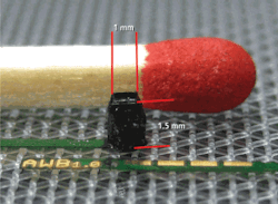
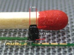
Awaiba’s standard product, the NanEye_2B, for example, features an array of 250 × 250 pixels and, while the imagers are fabricated at wafer level, the optics are assembled on the die in singulated form, allowing each customer to specify different lens configurations (see Fig. 1).
“Since this pick-and-place assembly method is used by CMOS manufacturers, the cost is competitive, especially if the yield per CMOS sensor wafer is low. In this way, lens modules can then be placed on top of good sensors, increasing the camera/wafer yield,” says Jyrki Saarinen, senior vice president and co-founder of Heptagon, a manufacturer of wafer-based lens modules. At present, this approach is especially favored by semiconductor vendors producing large volumes of miniature cameras for the consumer market.
Of course, both lens modules and CMOS imagers can be singulated from the wafer and cameras then built individually by combining lenses and imagers into a camera module.
Lens manufacturing
To create the lenses for these cameras, both direct etching and UV embossing methods can be used. In direct etching, a resist is first patterned onto a wafer and then reflowed to form hemispherical shapes. The wafers are plasma-etched and the hemispherical resist shapes are formed into the wafer material. After formation, multiple wafers can then be bonded together to form the wafer optic of the camera.
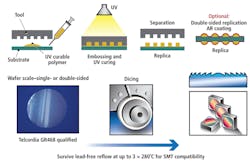
In UV embossing, a thin layer of liquid-phase epoxy material is spread onto a glass substrate. Then a lens mold is pressed against the epoxy layer so that the epoxy fills the microstructures within the mold. Hardening the epoxy through UV exposure then allows the resulting lens structure to be separated from the mold. Using this technique, Anteryon and Heptagon produce lens modules on a wafer, offering arrays of complete fully focused lens modules to subcontractors for bonding to imagers that form camera modules (see Fig. 2).
Many companies are also developing integrated autofocus functions for these lenses at the wafer level (see “Tunable Optics,” Vision Systems Design, July 2010). Here, many disparate techniques are being used to perform autofocusing that include electro-optical, electromechanical, thermo-optical, and acoustomechanical technologies. Samsung Electro-Mechanics, for example, is working on an electroactive polymer lens design where the thickness is controlled electrically. Others, such as Tessera, offer a MEMS-based solution using a spring-like silicon structure.
Through silicon
To reduce the size of cameras that use these lenses, wafer-level chip-scale packaging (WLCSP) of image sensors is required. Many of today’s CCD and CMOS imagers use dual-in-line packages (DIPs) that bond the I/O pins of the imager to a lead frame, but the resulting products are relatively large and must be through-hole mounted on a PCB.
To reduce the size of these devices while at the same time allowing them to be surface-mounted on a PCB, IC vendors offer ball-grid array (BGA) devices in which the IC die is connected to a laminated substrate either by wire-bonding or flip-chip technology. This laminated substrate then contains the solder balls that are attached to the bottom of the package for I/O.
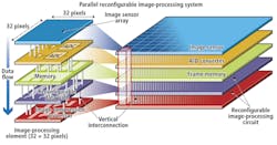
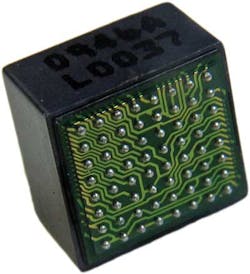
An alternative version of this packaging, known as through silicon via (TSV) technology, carries electrical I/O signals directly from the IC to the BGA substrate, eliminating the need for wire bonding and at the same time allowing a number of disparate ICs—including sensors—to be stacked in a 3-D fashion. Such an approach has been used by ZyCube in a novel 3-D image processor that incorporates an image sensor, A/D converter, frame memory, and reconfigurable image processor in a four-layer stacked TSV configuration (see Fig. 3). The company has also demonstrated a 3-D artificial retina using the same process.
Coupling to TSVs to create these 3-D stacks can be a challenging proposition, but a number of methods such as copper thermal compression (CuTC) and direct bonding can be used. CuTC uses temperature and pressure to form connections; processes such as direct bond interconnect (DBI) from Ziptronix allows connections to be made at CMOS-compatible temperatures.
Increased sensitivity
In developing their CMOS imagers, IC vendors are looking to increase sensitivity and improve quantum efficiency. To do so, many—including Toshiba, Aptina, Oki, STMicroelectronics, and Samsung—have turned to backside illumination (BSI) to achieve these goals. Rather than capture photons from the frontside of the die, BSI collects photons from the backside so that light enters the device unobstructed by the metal and dielectric layers of the device’s interconnect structure.
This involves thinning the backside of the wafer close to the photodiode level and placing the color filter and lenses on this wafer backside. Since light directly strikes the silicon, BSI can deliver superior low-light sensitivity and allows for shorter lens heights, which in turn enables thinner camera modules. When using BSI, TSV is not required because the contacts for the imager already exist on the reverse side of the silicon substrate. Omnivision uses BSI sensors manufactured in this way with Shellcase packages from Tessera.
When coupled with TSV packaging technology, BSI increases the image quality of the devices while decreasing package size.
Camera modules
Because of the intensely competitive nature of wafer-scale manufacturing, many manufacturers are unwilling to discuss which technologies they are using to produce miniature cameras. Despite this, these manufacturers are more than willing to promote their products once developed. A number of manufacturers including Jabil Circuit, STMicroelectronics, and Toshiba have announced products that reduce both the size and cost of cameras (see Fig. 4).
FIGURE 4. Jabil Circuit, STMicroelectronics, and Toshiba have all announced small camera modules that integrate CMOS imagers and lenses. (Image courtesy of Jabil Circuit)
These are all offered in different sensor formats and incorporate a variety of features. Jabil’s PW3625A embedded camera module measures 5.6 × 5.7 × 3.5 mm and features a 1600 × 1200-pixel CMOS imager, integrated signal processor, and wafer-level optics.
STMicroelectronics’ VS6525 VGA module also incorporates both sensor and optics and is offered in a 4.9 × 4.9 × 2.5-mm package. Toshiba’s TCM9000MD chip-scale camera module measures 4.00 × 4.00 × 2.23 mm and features a 648 × 492-pixel VGA CMOS imager that can operate at rates of 30 frames/s. Toshiba also offers a higher-resolution version of the camera featuring a 1648 × 1216-pixel CMOS imager that measures 6.31 × 6.41 × 4.35 mm.
Recently, Jerôme Baron of Yole Développement has reported that wafer-level processing of the optical lenses was provided to STMicroelectronics by Heptagon. Lenses for Toshiba’s camera modules were supplied by Anteryon.
According to Heptagon’s Saarinen, CMOS manufacturers and integrators have special interest in using wafer-level processes to start bonding lens-module wafers with their CMOS sensor wafers.
“Since these companies already have the experience of wafer-level processes, this would allow them to move forward in the value chain, allowing them to offer not only CMOS sensors but also cameras,” he says. And, according to Yole Développement’s Baron, the current rush toward WLC manufacturing will simplify the camera module supply chain, enhance overall integration, and reduce manufacturing costs.
Company Info
Anteryon Eindhoven, the Netherlands, www.anteryon.com
Aptina San Jose, CA, USA, www.aptina.com
Awaiba Madeira, Portugal, www.awaiba.com
Heptagon Rueschlikon, Switzerland, www.heptagon.fi
Jabil Circuit St. Petersburg, FL, USA, www.jabil.com
Oki Tokyo, Japan, www.oki.com
Omnivision Santa Clara, CA, USA, www.ovt.com
Samsung Electro-Mechanics Seoul, Korea, https://sem.samsung.co.kr
STMicroelectronics Geneva, Switzerland, www.st.com
Tessera San Jose, CA, USA, www.tessera.com
Toshiba Tokyo, Japan, www.semicon.toshiba.co.jp
Yole Développement Lyon, France, www.yole.fr
Ziptronix Morrisville, NC, USA, www.ziptronix.com
ZyCube Yokohama, Japan, www.zy-cube.com
Vision Systems Articles Archives
