Binning techniques increase signal-to-noise ratio in CMOS imagers

Andrew Wilson, Editor, [email protected]
Kodak Image Sensor Solutions (Rochester, NY, USA; www.kodak.com) continues to enhance its CMOS image-sensor portfolio with the release of 3- and 5-Mpixel sensors. Based on the company’s new PIXELUX technology, the image sensors can be operated in several binning modes to increase the sensitivity of the devices when used in different applications.
“In the development of these devices,” says Michael DeLuca, marketing manager for the Kodak Image Sensor Solutions group, “we leveraged CMOS pixel design intellectual property that Kodak has developed over several years.” The result is a series of devices based on a shared-pixel architecture that comprises four fully pinned photodiode sensing elements and a four-transistor readout (see figure).
“By covering part of the photodiode’s surface with the same semiconductor material as the substrate,” says Terry Guy, Kodak product marketing manager, “the surface potential is pinned to that of the substrate. The effect is to reduce dark current, reduce read noise, and increase blue quantum efficiency,” he says. To reduce the transistor-to-pixel ratio in the sensors, multiple transistors are shared across groups of four pixels, increasing the fill factor of the device and enabling charge-domain binning that can be used to increase the signal-to-noise ratio of the device.
“This expanded sensitivity is especially useful in low-light-level applications,” says Guy. In addition to reading out each pixel separately, these binning options include binning two or four pixels together. Because the binning architecture allows multiple pixels to be sampled in a single read operation, the frame rate is increased compared to standard off-array averaging. For same-color binning, this results in a 2X increase in frame rate; for all-color binning a 4X increase can be attained. According to DeLuca, such on-chip binning also results in improved sensitivity, lower noise, and reduced aliasing.
“In standard signal averaging,” he says, “each individual pixel is read and then averaged off of the array, so that the final signal includes the read-noise components from each pixel. PIXELUX technology allows the charge from multiple pixels to be measured in a single read operation, reducing the total noise in the final image and increasing the sensitivity of the sensor when it is operated in this mode.” The pixels can be binned either two at a time (same-color binning), or all four at once (all-color binning, resulting in a monochromatic image with very high sensitivity). The results of on-chip binning are dramatic (see photos).

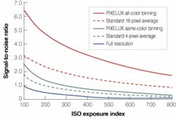
While reading data from each individual pixel at full resolution results in a normalized signal-to-noise ratio of 1.0 at ISO 100, using same-color binning results in a signal-to-noise ratio of approximately 2.5 at the same exposure level. When full all-color binning is used, this signal-to-noise ratio increases to 6.5 at ISO 100.
“Binning provides customers with additional benefits,” says DeLuca, “by offering camera designers an opportunity to increase sensitivity in applications that call for reduced resolution. Through binning, a megapixel sensor can be operated at video resolution with an overall increase in sensitivity, a key consideration for video capture.” For a VGA image sensor, for example, the full resolution may be 640 × 480 pixels. When two-pixel binning mode and averaging are used, this resolution will decrease by one-quarter. When all-color pixel binning and averaging is used, 1/16 monochrome VGA resolution results. “This all-color binning mode is especially useful when images must be captured at very-low-light levels and a high signal-to-noise ratio is required,” says DeLuca.
According to Kodak’s Guy, the company will use the fabrication facilities of IBM (Burlington, VT, USA; www.ibm.com) to manufacture a range of devices based on the technology. Although primarily targeted at low-cost consumer applications, these devices will also be used by those wishing to lower the cost of their machine-vision cameras.