Vision system simultaneously checks 2- and 3-D images of wafer bumps and flip-chip substrates.
By C. G. Masi, Contributing Editor
As microelectronic circuits get smaller, they present increasing challenges to all test-and-measurement modalities. Now, bumped-wafer/flip-chip technology is shrinking even package-feature critical dimensions (CDs) to the Rayleigh resolution limit for visible-light inspection. To ensure reliable chip/package interconnections, no inspection modality is better than automated inspection, but the technique requires a combination of 2- and 3-D inspections that lead to complex test strategies involving long inspection sessions on multiple stations. Aceris 3D, an inspection-equipment developer, worked with camera-manufacturer Adimec Electronic Imaging to develop a multicamera inspection head that unites 2- and 3-D measurement systems and makes the technologies work simultaneously.
Wafer bumps and flip chips are two sides of an advanced semiconductor packaging system. The traditional way to build semiconductor integrated-circuit (IC) packages is to bind the semiconductor device backside down on a substrate (lead frame), then use an automated wire-bonder to spot-weld wires from bond pads on the device to corresponding metal pads on the lead frame. The process, although highly automated, results in packages that are many times the physical size of the semiconductor device chip and that take an impractically long time to wire up.
For decades, IC manufacturers have been developing surface-mount packaging systems that have steadily driven down the footprint required to make reliable interconnections between semiconductor devices and the circuit boards that make them work. As each generation of package succeeds in shrinking intrapad dimensions, IC-device designers find a need to add more leads. Currently, devices sport up to 2500 leads packaged as tightly as 50 µm or less between bump centers.
BUMP FUNDAMENTALS
Each wafer bump is the connection point for a terminal in the underlying circuit (see Fig. 1). Bumps can be made of any conductive eutectic material, but are typically 35 to 50 µm high and 100 to 125 µm in diameter and made of gold. The bumps must be of uniform size and shape to ensure contact with their counterpart structure-the flip-chip substrate. Since wafers are a bulk-manufacturing structure containing tens or hundreds of individual circuits, completed wafers have to be broken up into individual “dies” that each carry the circuitry for one IC device (seeVision Systems Design, May 2006, p. 43).
“Flip chip” describes the method of electrically connecting the resulting die to the package carrier. The package carrier-the flip-chip substrate-then carries signals from the integrated circuitry on the die to the rest of the electronic circuitry outside the package. To make these connections, the manufacturer “flips” the bumped die, placing it face down with the bumps directly contacting corresponding bumps on pads on the carrier.
Bump shape is a 3-D measurement. That is, to determine each bump’s shape, the transverse dimensions of the bump must be measured in addition to the out-of-plane height. In many ways the height is more critical than transverse measurements because bump-height statistics determine whether all of the bumps will be able to make contact at the same time. Any undersized bump, for example, will fail to contact its carrier pad, while an oversized bump will interfere with all the other bumps making contact. Since any one contact failure will cause a device failure,all of the bumps must be of uniform size.
Simultaneously, an accurate bump-diameter measurement is needed. Given a uniform bump height, then bump-diameter uniformity provides an accurate estimate of bump volume. Bump volume is important to ensure a good connection.
The final step to mating die with carrier is heating them to the bumps’ eutectic temperature. At the eutectic temperature, the bump material begins to flow, wicking to all parts of the pad. If the volume of a given bump is too low, the material will not be able to fill the gap between the die and the pad. That connection will then fail, ruining the device. If, on the other hand, the bump volume is too large, the material will overfill the volume, shorting to the next pad and, again, ruining the device. With hundreds or thousands of bumps being connected at once, there is little or no chance of saving a failed device.
Measuring the bump
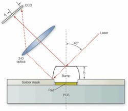
There are a number of ways to measure a bump’s height, including x-ray laminography and confocal scanning laser microscopy. Generally the fastest method is structured light. The Aceris process starts by rastering a laser beam over the bump, but the laser beam enters at a 45° angle to the wafer plane (see Fig. 2). The camera, which is actually a custom-built video microscope, observes the impingement spot (where the beam intersects the bump surface) as the laser rasters over the bump. If there were no bump, the spot would simply trace the raster pattern as a set of straight lines. Since the bump has 3-D shape, however, the lines appear bent or broken.
The spot intercepts the bump’s upper surface before reaching the wafer plane, offsetting the impingement spot toward the laser. The greater the height, then the greater the offset. The camera, which is an area-scan unit, sees and measures this offset as a function of position in the field of view (FOV), and the image-analysis computer computes the bump’s 3-D shape.
While this measurement technique provides very accurate and reliable height measurements, it cannot see the entire bump. It looks from only one perspective, so there might be a large hole on the other side that the structured-light system does not see. Although the laser-deflection system-which uses piezoelectrically driven mirrors to move the beam axis around-can move quickly, it does take significant time. Doubling or tripling the test time by taking views from different perspectives is not feasible in a production environment.
To solve this problem, Aceris mounts a second camera directly over the bump being inspected. This second camera, looking directly down, sees the entire bump outline in two dimensions. It then quickly spots any hole that the structured-light measurement missed.
Lighting
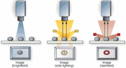
Different lighting arrangements bring out different parts of the scene-all of which provide necessary information (see Fig. 3). Episcopic (brightfield) illumination highlights the bump’s top. Side lighting provided by a ringlight set fairly high above the wafer surface highlights fiducials built into the wafer that help the system navigate. Finally, low-angle darkfield lighting provided by a ringlight set low near the wafer surface makes the bump’s equator show up like a glowing ring. That allows the system to ensure that the bump is properly shaped (so the analysis formula gives the correct volume).
Since grabbing the 2-D snapshots is much faster than carefully scanning the surface with a laser, there is time to capture many 2-D images. Thus, incorporating the three lighting systems, two cameras, and the laser into one vision head makes it possible to add all the 2-D imaging chores into the test sequence with no time penalty.
Aceris uses a red laser to do the structured-light measurement and green light to illuminate the scene for 2-D imaging. Color filters on the two cameras prevent the green light from confusing the structured-light camera and the red light interfering with the 2-D images. With the 3-D scanner head, Aceris can scan 20 to 40 300-mm wafers per hour with 0.08-μm effective resolution, which is below the Rayleigh limit. Using multiple scans and curve fitting in the analysis software, however, it can be done. Such sub-Rayleigh and subpixel analysis methods have been in use since the early 1990s.
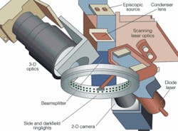
All the optical paths in the scanner head are folded to some extent. For example, the 2-D camera, which was optimized for Aceris by Adimec, looks in horizontally at a beamsplitter, which folds its optical path through 90º, so that it looks directly down through the ringlight’s center at the system’s field of view (FOV). The episcopic source looks down through a condenser lens and beamsplitter to illuminate the FOV, as well. Color filters on the camera apertures prevent interference between the 2- and 3-D imaging systems.
The ringlight structure has a lower row of LEDs to provide the darkfield lighting that highlights the bumps’ edges. A second LED row set higher up in the same structure provides side lighting to pick out fiducials marked on the wafer or substrate surface. These are important to ensure accurate registration between the 2- and 3-D imaging systems.
A laser diode for 3-D measurements sends its beam into a pair of piezoelectrically driven first-surface mirrors, which deflect it to the bumps under inspection in the FOV. This beam impinges on the wafer/substrate plane at an angle of 45º. The 3-D camera, also optimized by Adimec for Aceris, looks along an optical axis that makes a 90º angle with the laser beam. The laser axis, camera axis and surface normal all lie in the same plane to maintain the correct geometry (see Fig. 4).
Because the system performs its 2- and 3-D measurements simultaneously, and it takes less time to perform the 2-D tests than the 3-D tests, it can process wafers as fast as the 3-D system can go. As the FOV is 8.2 mm wide, it measures hundreds of bumps at a time. Piezoelectric scanning also contributes to system speed. Altogether, the head can measure more than 7500 bump profiles per second, making it possible to process 20 to 40 200-mm wafers per hour.
null
