ROI processing offers opportunities

Region-of-interest processing reduces the raw data fed into image-processing systems, speeds performance, and captures critical information.
By Mark Butler and Neil Humphrey
The best machine-vision cameras provide higher throughput and better image quality with more pixels and more bits, allowing ever-faster inspection for increased system throughput. But despite the growth of cheap computing power, inspection systems for applications such as electronics inspection are still frequently overwhelmed by the torrents of raw data output from advanced cameras.
One way to retain the high resolution, high bit depth, and high frame rates without choking the imaging system is to process only certain regions of interest (ROIs) from a complete image. ROI processing can allow one imager to satisfy diverse aspect ratio or resolution requirements for a range of applications, helping manufacturers maximize their return on investment in existing host-processing systems. ROI processing can be performed by the camera’s sensor either through partial scanning (CCD-based cameras) or windowing (CMOS-based cameras), or on the host system through effective use of FPGAs.
CCD Partial Scanning
CCD and CMOS imagers both collect light and convert it to electric charge. With a CCD, charge is shifted vertically row by row and then horizontally pixel by pixel toward one or more output nodes where the charge is converted to voltage, conditioned, and sent off-chip. The limited number of outputs on CCDs mean the output uniformity (important in image quality) can be very high, and the mature, optimized wafer processes used to produce CCDs usually deliver better noise performance than CMOS imagers can demonstrate. But to maintain the analog signal integrity necessary for a high-quality image, the throughput of CCDs is currently limited to 40-60 MHz per output by the capacitances of the bond wires and leads that convey the signals off-chip.
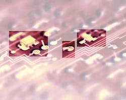
CCDs were the first imagers to offer ROI processing through partial scanning, which allows the camera to throw away the portion of the image that the designer is not interested in. With partial scanning, a CCD can read out a variable band from the central part of the imager. Keeping the image centrally located keeps the center of the image in line with the image center of the lens, minimizing distortion (see Fig. 1).

Partial scanning is accomplished by performing a number of consecutive vertical shifts into the readout register and discarding the charge signals instead of reading them out through the output node. Without the need to output each pixel in the row, the vertical transfers can be done quickly, which translates into an increase in frame rate because the sensor outputs fewer rows in each frame. Once the ROI is reached, the sensor is operated normally, outputting pixels in the appropriate rows. However, on-chip partial scanning is limited to the vertical direction only.
CMOS Windowing
CMOS imagers convert charge to voltage inside every pixel. This reduces the uniformity of response and often brings higher noise, both fixed and random, but allows some additional useful functionality. Pixel voltages are read out using column and row select circuits (similar to random access memory). Once the selected section of a row or column is read out, a new section can be selected and read out, and unlike with a CCD, the new selection does not have to be in any way related to the previous one (see Fig. 2).
Depending upon the architecture of the CMOS sensor, both vertical and horizontal windowing can be performed. In most designs, this allows a corresponding increase in frame rate, since pixel signals are sent in parallel through a bank of column amplifiers, followed by column A/Ds, and finally into a high-speed multiplexer that sends the digitized data off chip. The integration of many parallel on-chip A/Ds in a CMOS chip can allow for high pixel clocks (thanks to digital output) with high frame rates (due to parallel architecture). Today, there are several examples of megapixel and larger CMOS chips running at 1000 frames/s.
A high-speed camera such as the DALSA CMOS-based 4M60 Stop Action requires Medium Camera Link (320-MHz throughput) to accommodate its full resolution and frame rate. But if the system integrator is only interested in part of the field of view, the camera bandwidth to base Camera Link (160 MHz) could be limited by using windowing to reduce the total image information acquired (that is, the 2352 × 1728 image could be windowed to 2352 × 864). The end benefit would be a reduction in the number of cables required and a reduction in information for less complexity in back-end processing.
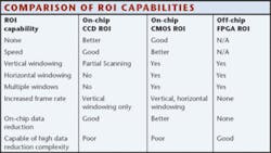
Windowing with CMOS sensors can extend beyond a single window to multiple windows by properly addressing the correct rows and columns of interest. With multiple windows or ROIs, the end user can maximize sensor output bandwidth with useful information. This, of course, assumes that the system frame grabber can communicate with the camera and interpret the multiple windows properly.
Off-chip ROI Processing
Another type of ROI processing is done through off-chip (off-sensor) processing, typically through an FPGA or DSP. This can be done in the camera or on the frame grabber. In this case, the FPGA performs image-based algorithms to process the image and then provides only the important information. In some cases, the raw data are reduced to a pass/fail notice. In other cases, the algorithm crops the image or strips away background information from unimportant regions.
The drawback is that this does not improve imaging throughput because the sensor must still output all its raw data before ROI data reduction begins. In-camera processing can reduce the camera-to-frame grabber bandwidth requirements, but it can also increase the camera-to-frame grabber communication complexity. Locating the FPGA in the frame grabber instead of the camera removes any camera-imposed limit on the number of windows and reduces camera complexity (and cost) but offers no improvement in imaging throughput.
Real-World ROI Application
One example of the need for on-chip ROI is in 3-D laser profiling for solder paste inspection. In this application, a laser line is projected onto a circuit board and its scatter pattern is measured by a camera. Using the 4M60 camera, the ROI could be reduced to 2372 × 100 (23.7:1 aspect ratio) to accommodate the laser’s narrow focus while significantly increasing the camera speed from 62 frames/s (at 2352 × 1728 resolution) to close to 1000 frames/s with the reduced ROI.
It should be noted that area cameras are not the only devices that can serve such an application. Three-dimensional laser profiling ideally requires an even larger aspect ratio, which wastes most of an area camera’s vertical resolution. A significantly more cost-effective solution with even higher resolution and throughput is a TDI sensor operated as an area device. This is possible with most TDI sensors by proper control of horizontal and vertical timing clocks. TDI aspect ratios can be very high; for example, a DALSA high-speed 8192 × 96 TDI camera operated in area mode has 8k resolution with an aspect ratio of more than 80:1 and a frame rate of approximately 700 frames/s.
ROI processing can help improve inspection throughput and quality without increasing the processing bandwidth requirements. On-chip ROI processing allows for frame-rate improvement and potentially throughput improvements, while off-chip ROI does not provide frame-rate improvement on the raw data but is independent of camera functionality. CMOS technology has other on-chip reduction benefits through the addition of horizontal windowing and multiple windows. Any ROI solution provides a mechanism to reduce the raw data fed into systems.
MARK BUTLER is product manager and NEIL HUMPHREY is manager of corporate publications at DALSA, Waterloo, ON, Canada; www.dalsa.com.