Vision helps dice wafers into chips

Scribe-and-break method turns semiconductor wafers into integrated-circuit chips.
By C. G. Masi, Contributing Editor
The usual method of subdividing (or dicing) semiconductor wafers is to cut them up with a diamond saw. It is a very precise but dirty and wasteful process. To keep the saw blade cool, operators have to flood the wafer surface with a liquid slurry, which carries away both heat and ground-up particles. The blade has a significant width, leading to a “kerf,” or strip of material that the saw grinds to powder.
That process is fine for relatively inexpensive silicon material used to make electronic components covered by protective passivation layers. It cannot, however, be used to make many advanced semiconductor devices-either because the devices cannot stand up to the slurry or because they are made of exotic material such as gallium arsenide (GaAs), which is too expensive to grind up. For such devices, scribe-and-break is the only method. To be a viable manufacturing method, however, automated equipment is needed.
Jeff Atkinson, principal at equipment-maker SurvUs, had a number of ideas for more precisely controlling the wafer-scribing process. While he had experience dicing wafers, his expertise with automated manufacturing equipment and especially machine vision was limited. He called on precision-system designer P. C. Lindsey, president of Micro Processing Technology (MPT), for help with his ideas. Lindsey saw that using machine vision and robotics would make it possible to not only improve process control but also fully automate the scribe-and-break system.
“There are two other companies that make scribe-and-break systems right now,” Lindsey says. “Both those companies have tried to include the scribe and the break in the same machine, and, in doing that, they compromised both processes.”
System Concept
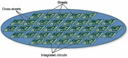
Since scribing and breaking the wafers were two separate steps performed in sequence, it made sense to design two separate machines to work asynchronously. The first machine (the scriber) marks the wafer to be diced along the “streets,” or spaces, between the individual circuits patterned on the surface (see Fig. 1). Streets on wafers intended for scribe-and-break typically range from about 20 to 50 µm in width. Streets intended for diamond sawing must be considerably wider-in the 150- to 200-µm range.
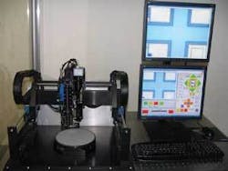
The second machine (the dicer) breaks the wafer into individual chips. Machine vision plays a significant role with the scriber, but not the dicer. The scriber machine consists of a scriber head mounted on a gantry over a rotary stage (see Fig. 2). The scriber head includes the vision system’s microscope and camera and a force-feedback system that touches the scriber tip down with just enough pressure to scribe the line (see “Getting the scribe line right,” p. 46).
Alignment is key to accurately scribing lines. Before putting a production wafer on the stage, it is important to align the vision-system coordinates with the scriber’s direction of travel as defined by the gantry’sx (left-right) axis.
The scriber system has an automatic alignment routine that uses a test wafer made of the same material as production wafers, but with no ICs patterned onto it. The system touches the scriber down onto the test-wafer surface and runs a scribe line between predetermined start and end points in motion-control coordinates. The system then looks at the scribe line through the camera and calculates any translational and rotational offsets needed to match vision-system coordinates with machine coordinates.
With the scriber head aligned, the processing of production wafers can begin. Wafers are held in position via a “vacuum chuck,” which is a circular plate of sintered ceramic material. A vacuum pump pulls air out of the space between the wafer’s underside and the vacuum chuck’s upper surface so that outside air pressure will hold the wafer in place.
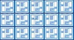
The vacuum chuck mounts on a rotary stage. The scribing process proceeds in two steps for each wafer. First, the wafer must be aligned to the machine coordinates so that the scriber can incise straight lines down each street with one movement of the gantry along itsx axis. At low magnification, the vision system locates several dies in the field of view via pattern recognition, then calculates a rotational offset (see Fig. 3). The rotary stage then adjusts the wafer orientation so the streets align with the gantry well enough that the gantry can slew from one end of a street to the other, and still have the street in the camera’s field of view at high magnification.
The system takes note of where the street ends appear in the field of view. The vision software can use the vertical offsets to calculate a finer rotation correction. With this second correction, the gantry can draw the scriber from one end of a street to the other while keeping the scribe line within 1 µm of the scribe-street centerline.
The system is then ready to scribe all of the lines along one direction. It moves the scribe head to one end of the topmost street and positions the scriber tip over the starting point. It then drops the tip to the wafer surface and draws it across the wafer until it reaches the other end of the street. It lifts the tip, moves one “block” in the y direction to find the start of the next street, drops the tip, and scribes the next street.
The system repeats the step and scribe process until all the streets in that direction are scribed. To scribe the cross streets, the system rotates the rotary stage 90° and goes through the wafer-alignment and scribing process again for all those streets. The result is a wafer with all streets-in both directions-scribed and ready for breaking.
Vision Architecture
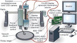
The optical system consists of a Navitar microscope body with a 1.5X objective, 12X zoom adapter, and a 2X projector lens. The image sensor is a Scorpion 1360 × 1024 progressive-scan color CCD camera manufactured by Point Grey Research. The microscope body allows episcopic illumination via a 13-LED Navitar source.
The camera sends its images to the host computer via an IEEE 1394 (FireWire) link to a National Instruments PCI-8252 frame-grabber board. Lindsey chose to use FireWire, rather than another protocol such as Camera Link, largely because the FireWire cable is lighter and more flexible (see Fig. 4).
“It means there’s less influence on the gantry by the wire bundles,” he says. “If you have a bunch of really heavy wire bundles, it tends to affect gantry movement.”
The host computer also carries a National Instruments PCI-7358 motion-control board. This unit provides eight motion-control channels, which is enough to run the entire mechanical system. The host computer is a custom system made by a local computer shop to Lindsey’s specifications. It runs Microscoft Windows XP operating system with application software that Lindsey wrote in National Instruments’ LabVIEW environment.
He used the company’s Vision Development Module to program the image-acquisition and processing functions and their Motion Development Module to program the motion control functions.“ The system is fully automated,” he points out, “but you have to have maintenance screens, an operator interface screen to show them what’s going on, and a screen available for technicians to do things manually if necessary.”
The system includes two 17-in. LCD displays. One of them displays the camera output, and the other is the operator-machine interface. “Having a dedicated vision display allows technicians to get a very large, clear image of what the camera and the microscope are seeing,” Lindsey says.
MPT is now turning the scribe-and-break system into what it hopes will be a standard product used throughout the MEMS and compound-semiconductor IC industries. The company has installed the prototype scriber machine at Skyworks Solutions’ GaAs fabrication facility.
“The company is experiencing a big increase in demand for their devices and needed to increase their scribe-and-break output fairly quickly,” Lindsey reports. “They’ve been running the system 24/7.”
Features, advantages, benefits

“This is the wafer scriber that I have dreamed of having for years. For the first time I can set up a scribe process for a specific force and know that value will be the same the next day or a year from now,” says Jeffrey Atkinson, principal at SurvUs. “The use of machine vision in the system makes operators significantly more productive. Rather than sitting in front of the scriber to align the wafer and monitor the process, they can be mounting wafers, entering log data, and packing up wafers for shipment.
“The precise scribe positioning and force control allow us to run the system at a faster scribe speed than others we have tried. Depending on the material being scribed, our material throughput is three to six times higher. Overall, we are exceptionally pleased with the results,” he adds.
Getting the scribe line just right
“You have to have extremely good force control when you’re doing the scribe process,” P. C. Lindsey, president of Micro Processing Technology, points out. Different materials require different forces to scribe properly. Too much force causes the scriber to dig in and gouge material from the surface. The material then forms particles that contaminate the process. Applying too little force leaves too light a scribe line to guide the break. Just enough force creates plenty of strain to guide the break, but does not penetrate the surface and break off material.
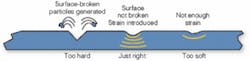
“We’ve developed a force-feedback apparatus,” Lindsey continues, “that senses the force on the scribe tip and corrects it using computer feedback 4000 times a second.” Scribing GaAs, for example, requires 2 to 5 g of force. The feedback system maintains the stylus force within a tenth of a gram of the set point, while the tip traverses the wafer surface.
Company Info
Micro Processing Technology
Lafayette, CA, USA
www.microptech.com
National Instruments
Austin, TX, USA
www.ni.com
Navitar
Rochester, NY, USA
www.navitar.com
Point Grey Research
Vancouver, BC, Canada
www.ptgrey.com
Skyworks Solutions
Woburn, MA, USA
www.skyworksinc.com
SurvUs
Sebastopol, CA, USA
www.diamond-scribe-dicing-survus.com