New tools ease FPGA programming

FPGA programming tools allow system developers to rapidly embed image-processing algorithms.
By Andrew Wilson, Editor
Developers of high-performance frame grabbers and image-processing boards have sought to optimize the throughput of their products using dataflow architectures inherent within FPGAs. To optimize image-processing algorithms most effectively, developers often tailor their algorithms in hardware description languages (HDLs) such as Verilog and VHDL. Once described in this way, the programs can be compiled into register-transfer-logic net lists, synthesized into logical gates, then placed and routed and embedded into the FPGA.
For many, however, the task of programming in HDLs requires a steep learning curve and one that may add many months of labor to a machine-vision or image-processing design. Because of this, a number of companies are now offering image-processing libraries that run on FPGA-based boards that can eliminate programming in HDLs.
Easier to use
“Now,” says Reuven Weintraub, president and CTO of GiDEL, “the maturity of electronic-system-level (ESL) design tools for FPGAs, coupled with demand for real-time performance in imaging and video-based applications, has turned designers to programmable logic to provide coprocessor acceleration for existing DSP or microprocessor solutions. Processor-intensive functions are offloaded to the FPGA, processed in real time, and returned to the host or migrated completely to the FPGA.”
Although these tools may not offer the ultimate performance of a finely tuned algorithm for a specific FPGA, they do offer a means for system developers to deploy code on FPGA-based frame grabbers and image-processing boards, while at the same time reducing possible time-to-market of the systems. Furthermore, because these tools provide a certain level of hardware abstraction, they do not require that the system’s developer understand the low-level timing and communications protocols between on-board hardware components. Rather, because such high-level interfaces have been developed on specific frame grabbers and image processors, they leverage the low-level drivers and application programming interfaces (APIs) already developed by hardware vendors.
At the 2005 VISION Show (Stuttgart, Germany), Silicon Software introduced a graphically oriented interface called VisualApplets that lets developers program machine-vision and image-processing functions on the company’s Xilinx Spartan IIe-based microEnable III PCI Camera Link frame grabber (seeVision Systems Design, Jan. 2006, p. 48). Rather than use a VHDL compiler, these prewritten image-processing functions are transparently converted into an FPGA layout using Xilinx’s place and route software and then executed.
Rapid development
At the 2006 Vision Show East (Boston, MA, USA), GiDEL showed how its range of Altera-based PC development boards and interfaces could be used running the Simulink environment from The MathWorks. According to Weintraub, GiDEL has taken both an ease-of-use and high-performance approach to FPGA systems development. “To rapidly implement image-processing algorithms,” he says, “GiDEL’s PROC_HILs software requires no understanding of the underlying hardware. It automatically builds dedicated acceleration hardware for users’ Simulink designs.”
Using the PROC_HILs tool enables the developer to download the Simulink design into one of the company’s FPGA-based processing boards and simulate it, while the design runs on the on-board FPGAs, communicating with Simulink in real time. “By operating the added GiDEL PROC_HILs object to the design, an HDL code is automatically generated from the Simulink design and synthesized and compiled to an FPGA binary file that is compatible with the processing board,” says Weintraub (see Fig. 1).
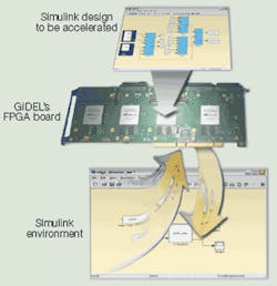
“After generation, a new Simulink design is created containing an HIL block including all the inputs and outputs of the original design. This HIL block automatically loads the FPGA binary file to the board and performs all the necessary communications to execute the design in hardware,” Weintraub continues. To date, the company offers a number of PCI-based add-in boards including its PROCStar II that supports up to four Stratix II FPGAs. Daughterboards that support Camera Link and DVI input and output are also available.
With GiDEL PROCWizard, performance can be accelerated even more. A user can generate an application driver (a C++ class) for each application that operates directly from the user’s software program.
Custom triggering
National Instruments also offers reconfigurable I/O hardware (RIO) in the form of its R Series of data-acquisition modules, CompactRIO platform, and Compact Vision System (see Fig. 2). With the computer-vision system’s on-board gate arrays, developers can design custom FPGA logic to add custom triggering, motion control, or custom communications protocols to machine-vision applications.
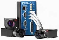
To support these products, the company’s LabView FPGA software allows custom I/O and control hardware to be created without prior knowledge of traditional HDL languages or board-level hardware design. Using the LabView FPGA module, the LabView graphical development system can reconfigure the on-board FPGA to customize measurement and control hardware and integrate RIO hardware within a LabView application. Independent software vendors are also realizing the power of adding such functionality to third-party hardware.
At the Vision Show East, for example, Celoxica introduced more than 140 image-processing library functions called PixelStreams. When used in conjunction with the company’s DK Design Suite, the graphical editor can call and develop C-based image-processing functions and provide direct C-to-FPGA synthesis. In June 2006, Celoxica partnered with GiDEL to integrate Celoxica’s ESL design environment and video IP libraries with GiDEL’s FPGA+ modular DSP platforms.
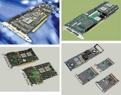
Using PixelStreams, systems can be developed by incorporating library functions from the user’s C-based code or automatically generated from the PixelStreams editor. “At present,” explains Celoxica’s Simon Johnson, “the company currently supports hardware products such as the Anaconda from DALSA, the Tsunami from SBS, and all of GiDEL’s boards (see Fig. 3).
High-speed boards
DALSA’s Anaconda combines image-acquisition functions with a configurable FPGA and user-programmable PowerPC. At the core of the Anaconda board is an image-processing unit that allows developers to implement algorithms directly in hardware. This is composed of user-configurable FPGA hardware, general-purpose RISC processor, and an optimized memory architecture. As well as software development support from Celoxia, DALSA provides its Sapera LT software for acquisition and control, FPGA development specifications, and image-processing libraries for the PowerPC enabling application development on Windows 2000/XP computers.
SBS (now part of GE Fanuc) uses Altera’s Stratix EP1S40 FPGAs coupled with SRAM and SDRAM in its TS-PCI A40, a PCI-based FPGA frame grabber/processor. The TS-Series architecture, integrated with the SBS Wave FPGA toolkit software provides developers with an API, drivers, memory controller, and source code. To digitize images using the board, developers can opt to add interface mezzanine I/O boards for Camera Link and LVDS signals.
Matrox Imaging has developed its own FPGA developer’s kit for programming FPGA devices on Matrox Imaging hardware. “Images are growing in size and depth, so there is a surging demand for pixel pre-processing and fast algorithms for processing-intensive vision applications,” says Dwayne Crawford, product manager at Matrox Imaging. “Today’s FPGA devices offer an excellent means to offloading or accelerating image-processing tasks from the host PC.”
The Matrox FPGA developer’s kit (FDK) is intended for use with the Matrox Solios frame-grabber family and the Matrox Odyssey Xpro+ vision processor. The FDK features ready-built design components, productivity tools, and an optional version of Altera’s Quartus II 5.1 for Windows 2000/XP. Using the package, developers can select which image processing functions to offload from the host.
To develop a new board capable of performing FPGA-based imaging functions, however, requires intimate knowledge of the underlying hardware. For these customers, Celoxica offers a Platform Abstraction Layer that provides a consistent API for board-level C-based hardware implementations and a Platform Support Layer that provides hardware-specific support for the DK Design Suite.
Company Info

null