CMOS cameras find a niche
In applications that demand high speed and high dynamic ranges, CMOS cameras can outshine their CCD counterparts.
By Andrew Wilson, Editor
While CCDs remain the imager of choice for high-fidelity image capture, CMOS imagers present the system developer with a number of advantages, such as digital readout, on-chip programmability, and region-of-interest (ROI) image processing. Thus, while CCD imagers remain dominant in many machine-vision systems, CMOS imagers are gradually carving niche markets in low-cost consumer cameras, as well as in applications where high speed and high dynamic ranges are required.
Take one look at the specifications that distinguish CCD and CMOS cameras and their differences become apparent. Indeed, in choosing whether to use a CMOS or CCD camera for any given application, such parameters should be carefully studied because they provide information about both the imagers used and the cameras themselves. These parameters include the types of sensor used, spectral response, dynamic range, uniformity, frame rate, and windowing capability.
While many people initially touted CMOS imagers as low-cost replacements for CCDs, their design and fabrication have been more difficult to realize than once imagined. While CCD imagers that use photodiode arrays to convert photons into an electric charge, CMOS imagers use specialized fabrication methods that must be finely tailored. Because of the complexity required to do this, only a few very large manufacturers such as Cypress, Kodak, and Micron Technology currently offer these devices.
Camera specs
To understand whether a specific CCD or CMOS camera will meet the requirements of an application, system designers should study the spectral response of each camera. This provides a measure of the camera’s response to radiation at a specified wavelength. Such a spectral response is generally measured across the 100-1100-nm range.
Unfortunately, trying to compare the spectral sensitivity of individual cameras is not straightforward. Many camera vendors do not specify these parameters on their data sheets, and, of those that do, some specify the spectral response of the sensor itself, borrowing data from semiconductor vendors. Worse, there is no established standard for measuring this performance. How, for example, was the camera illuminated and what type of lens and lighting were used? Luckily, the EMVA has launched an initiative known as the 1288 standard to define a unified method to measure, compute and present specification parameters for cameras and image sensors used for machine vision applications.
By comparing the spectral characteristics, however, integrators can understand the performance differences between CCD- and CMOS-based cameras (see Fig. 1). The spectral response graph for QImaging’s Retiga EXi Fast 1394 digital CCD camera, for example, features enhanced visible and IR quantum efficiency resulting in a sensitivity designed for demanding low-light and fluorescence imaging applications. JAI Camera Solutions uses a CMOS device in its PC-640CL, so its VGA CMOS camera produces a different spectral response that is sensitive to near-IR. A similar spectral response can be obtained using the Retiga EXi by removing the IR filter.
More sensitive
One of the most important aspects of both CCD and CMOS camera performance is sensitivity, a measure of signal strength relative to background noise. This dynamic range is usually measured in decibels (dB) and calculates the background noise of both the image sensor and the readout electronics. DALSA’s 62-frames/s, 2352 × 1728 × 8- or 10-bit CMOS-based 4M60 SA, for example, features a dynamic range of 56 dB and uses a global shutter to eliminate image smearing or time displacement artifacts associated with full-frame, frame-transfer, or rolling-shutter cameras.
Two signal types can reduce the performance of an image sensor. While dark current is repeatable and can be removed either in an analog or digital fashion, shot noise is random and cannot be removed.
Perhaps the most popular method for removing dark current noise is correlated double sampling (CDS). CDS both calculates the difference between the reference and data levels of the CCD or CMOS signal and reduces some associated noise components. By taking two samples of the output of the imager and subtracting them, any noise source that is correlated to the two samples will be removed. This process can be performed both on- and off-chip. While incorporating CDS on a CCD imager is difficult, such additional circuitry is more easily accomplished with CMOS imagers.
CDS also can be performed off-chip using off-the-shelf CDS circuits from companies such as Philips Semiconductors and Analog Devices. These are most often used in CCD camera designs to reduce noise and increase the camera’s signal-to-noise ratio. In the design of its HR1100 and HR-200 CCD camera series, for example, Imaginant has used Philips’ TDA9965, clamp-track-hold circuit, programmable gain amplifier, 12-bit ADC, and a reference voltage regulator.
While cameras such as the FastCamera13 from FastVision have been developed for the high-speed analysis market, Imaginant’s HR-1100c CCD camera is a 2.5-frames/s unit squarely aimed at scientific markets where 4032 × 2686-pixel, 12-bit images need to be captured with a dynamic range of 60 dB (seeVision Systems Design, September 2005, p. 16).
Although CDS functions can be performed in the camera, other functions such as flat-field and defective-pixel correction must be used to correct for any variation of pixel values across the imaging array. To do this, camera vendors such as Imperx offer the integrator several software-development tools (seeVision Systems Design, July 2006, p. 20).
By computing a histogram of each pixel’s intensity across the array, the percentage difference of each pixel compared with its ideal flat field value can be determined. The camera can then compensate for each individual pixel value as images are captured by the imager. To correct for defective pixels across the array, the camera is uniformly illuminated and a defective pixel map file created. Allowing the developer to upload pixel maps for flat-field and defective-pixel correction ensures that the camera will perform optimally in a range of illumination conditions.
Higher range
While the dynamic range of CCD cameras is often greater than CMOS-based cameras, a number of companies such as Neuricam, Cypress, and Photonfocus have successfully developed CMOS devices and cameras that use logarithmic or logarithmic-like responses (seeVision Systems Design, October 2002, p. 37). In these devices, voltage response is presented as the logarithm of the light intensity.
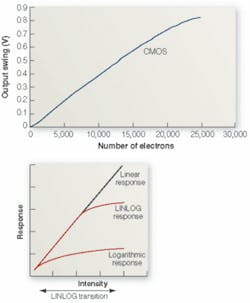
In the design of its MegaCamera SI-6600, for example, Silicon Imaging uses a portrait-style 6.6 million-pixel CMOS image sensor that is light sensitive between 400 and 1000 nm. By charting the pixel response curve in linear response mode, the relation between the electrons detected in the pixel and the output signal can be visualized (see Fig. 2). As can be seen, an increase in the number of electrons generated in each pixel will result in a roughly equal increase in output signal. Such linear increases are especially useful where absolute intensities need to be measured in applications such as photometry or image calibration.
For relative-contrast measurements, however, devices that incorporate a logarithmic response may be a better choice. These devices allow orders of magnitude of illumination levels to be compressed at the output range and produce dynamic ranges often in access of 120 dB. A number of companies, including Photofocus, Neuricam, and Vector International, now offer cameras based on these types of devices.
Developed at the Swiss Federal Institute of Electronics and Microtechnology, Photonfocus has further developed its LinLog technology and incorporated it into a number of cameras. Using a linear response at low illumination levels and logarithmic compression at high intensities increases the sensitivity of these cameras and results in a dynamic range of 180 dB.
One of these cameras, the Photonfocus MV-D1024, uses a progressive-scan CMOS imager with global shutter to achieve speeds up to 150 frames/s with a dynamic range of 120 dB. While these cameras are useful in robotics control, traffic management, and welding applications, camera vendors often recommend CCD-based cameras for microscopy, scientific-imaging, and medical-imaging applications.
Other companies also have integrated logarithmic CMOS imagers into their cameras. Vector International, for example, uses the Fill Factory (now Cypress) CMOS integrating active Lupa 1300 sensor in its FCm-1300 CMOS Camera Link camera to achieve 450 frames/s at 1280 × 1024 with a 100-dB dynamic range. Other companies such as Neuricam use proprietary image sensors. The company’s CLinkCam VGA camera is based on the its Pupilla sensor, a 640 × 480-pixel (VGA) gray-scale array that delivers 120 dB of dynamic range on 10-bit output with logarithmic response. According to Neuricam, the current version of the camera can acquire full VGA frames at 24 frames/s, while quarter-VGA frames can be captured at 96 frames/s.
Regions of interest
For many, the major benefit of CMOS-based cameras over their CCD counterparts is the capability to perform random vertical and horizontal windowing. While CCD-based cameras can operate in a partial-scanning mode that is limited to the vertical direction, CMOS-based cameras have no limitation. This can be beneficial where multiple imaging functions must be performed on different areas of the image, in predictive imaging where the results of image processing in one window can be used to control the processing functions of another window, or in high-speed imaging where ROI processing frame rates can be increase dramatically. Adimec’s Camera Link-based 4050m 4-Mpixel camera, for example, is a CMOS-based camera that operates at speeds up to 140 frames/s and features programmable ROI processing and asynchronous image capture.
Unlike CMOS-based imagers, however, it is more complex to fabricate readout electronics on exotic materials used in IR focal-plane arrays (FPAs). In cameras based on such devices, signals from each detector site on the FPA are read individually using a readout integrated circuit (ROIC) that is flip-chip bonded to the sensor. While many ROICs simply read all the information from the FPA, Nova Sensors recently announced its Variable Acuity Superpixel Imager (VASI) technology that allows ROI processing to be performed with IR imagers (seeVision Systems Design, July 2006, p. 22).
VASI technology allows windows within an IR image to be sampled at high spatial resolution, while the remainder of the field of view (FOV) is sampled at lower resolution. This guarantees that information content is preserved, ensures the total FOV is always monitored, and at the same time achieves variable frame rates.
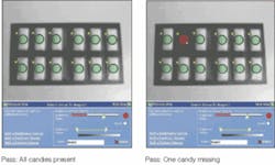
ROI processing has also been incorporated into products such as the Cognex Checker camera. Designed to replace and augment multiple photoelectric sensors, the camera uses ROI processing to allow developers to setup multiple “sensors” across the FOV of the image (see Fig 3).
Realizing the potential benefits of CMOS technology, many camera vendors now offer developers the choice of CCD- or CMOS-based cameras. While this means more choice for the systems integrator, there is as yet a lack of any method to measure, compute, and present specification parameters for cameras and image sensors used for machine-vision applications. Let’s just hope that the current work of the EMVA 1288 committee alleviates this problem.
Company Info
null


