Trends in CMOS and CCD image sensors
Developments in both CCD and CMOS imagers are opening new applications.
By Martin Wäny
For years, CCD and CMOS imager vendors have argued the merits of each particular process technology. However, for machine-vision applications, CCD imagers remain the detector of choice, while CMOS imagers are being used in more specialized applications requiring high speed, low cost, random access, or high dynamic range. Many of the reasons for this lie in the specific design of the pixels and readout electronics associated with each particular device.
In a CCD sensor, for example, charge is collected by an array of electrodes (gates) and then clocked to a common readout. In CMOS image sensors, charge-capture-and-transfer architectures are more varied. Some of the first CMOS image sensors featured photodiode arrays with a passive network of switches sequentially connecting each photodiode to a readout amplifier. In the late 1990s, an active element was used in each pixel and a voltage or current readout used to transfer the data.
In recent years, to increase pixel area and reduce kt/C readout noise at decreasing full-well capacity, charge-transfer architectures similar to those used in CCDs were used in buried channels inside CMOS image sensors. These technological developments are the most important reason why for consumer electronics and mobile-communication devices CMOS image sensors took the lead over CCDs.
This development also decreased the difference in responsivity between CMOS and CCDs. Today’s mainstream CMOS consumer image sensors use so-called “pinned” photodiodes and share one readout structure for two, four, or even 16 pixels. In such architectures, electrons are collected in a potential well and transported to a readout structure common to several pixels. This gives CMOS image sensors CCD-like advantages such as low dark current and correlated double sampling (CDS) and disadvantages such as limited full-well capacity and incomplete pixel reset (or image lag). Such architectures helped CMOS image sensors to reduce the size of each pixel to such an extent that 1.8-µm pixel pitch is now a reality.
Small pixels common in megapixel cameras produce a surprisingly low equivalent electron to readout noise ratio. This might sound impressive at first glance; however, the low equivalent noise in electrons usually has no advantage for machine-vision applications-most often the opposite is true. For example, a 2.8-µm pixel will produce ten times fewer photons than a 9-µm pixel. Further, the smaller the pixel, the lower the full well capacity, reducing signal-to-noise ratio. And, as consumer mainstream sensors are built with smaller and smaller pixels, they will be used less and less in machine-vision applications.
Machine vision
Machine vision is a small-volume market that has depended, to a large extent, on semiconductor technology developed for larger-volume markets. For the typical video-rate machine-vision application, this means that product costs have steadily declined. In the consumer field, established CCD vendors reacted to the declining costs of cameras by providing highly integrated companion chips that make it feasible for an increasing number of companies to build CCD cameras.
CMOS image sensors play a less significant role in machine-vision systems. This is because consumer-derived CMOS sensors usually feature a rolling shutter, which makes them difficult to use where pulsed illumination or fast-moving objects must be captured. Further, consumer cost pressures forced CMOS image sensor vendors to drive prices as low as $1 per device and thus to pursue ever-smaller pixel sizes. With 1.8-µm pixels, it’s no wonder why designers of machine-vision cameras question the necessity of producing so much data with so little resolution. However, there is a significant segment of machine-vision applications that requires higher performance from image sensors than consumer devices will deliver. Some CCD and CMOS manufacturers have realized this opportunity and optimize their production for added-value niche markets.
Increased complexity
CMOS imagers benefit from semiconductor-technology developments that allow the complexity of the imager and pixel structure to be increased without decreasing the optical fill factor. Novel photodiode designs can also reduce the dark current of CMOS sensors, such that dark current leakage becomes insignificant when the sensor runs at more than 30 frames/s.
Deep-submicron CMOS processes that allow 4-GHz processors to be used also can be tailored to manufacture faster image sensors. With state-of-the-art technology, high-speed image sensors can be made highly integrated, such that data can be transferred directly over high-speed serial digital-data interfaces, eliminating hundreds of parallel digital-data lines or banks of ADCs.
These technologies are being used for both area- and linescan sensors. Linescan sensors are typically used in high-speed applications, and CMOS linescan sensors are now emerging with all the support electronics placed beside each pixel, allowing 100% fill factor. For these CMOS sensors, each pixel becomes its own charge integrator and CDS amplifier, working in parallel. This permits the pixel area to be decoupled from the charge-conversion gain, allowing CMOS linescan sensors with relatively large pixel area but high conversion gain to be developed.
Such devices are challenging CCD-based time-delay-integration architectures that required complex triggering. The CMOS sensors also operate at high scan rates without increasing light intensity. Basler, for example, showed a 120-kS/s 4k linescan-based camera at VISION 2006 in Stuttgart, Germany (see Vision Systems Design, February 2007, p. 8).
Given the developments in semiconductor design software and manufacturing technology, application-specific sensors optimized for one application can easily be designed and fabricated reducing the overall cost and complexity even for small volumes. Depending on the added value in the application, these CMOS custom designs can be viable for 500 units per year or less.
CMOS and CCD
Many scientific, medical, and security imaging applications demand low-light solid-state sensors with photon-counting sensitivity that can capture hundreds of frames per second. Although currently available CCDs are capable of high quantum efficiency, low dark current, high linearity, and uniformity, the serial readout of conventional CCD designs limits their readout speed. In addition, the on-chip output amplifiers of the devices need to be operated at high speed, increasing CCD read noise, a factor that compromises CCD sensitivity when used in low-light-level applications.
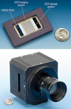
To overcome these limitations, engineers at Fairchild Imaging have developed a low-light-level digital camera with a Camera Link interface that combines the best features of CCD imagers and CMOS technology. The camera, shown at Photonics West (San Jose, CA, USA; January 2007), uses two CMOS readout ICs (ROICs) that are bump-bonded to a split-frame transfer CCD. Each ROIC is an array of capacitive transimpedance amplifiers (CTIAs) that connect to the CCD columns via indium bumps (see Fig. 1). Unlike conventional CCD devices, the CCD used in the Fairchild camera does not have any on-chip amplifiers. In operation, charge from each column of the CCD is transferred across the indium bump bonds and onto the CMOS ROIC, where it is converted to a voltage and amplified by the CTIA.

By eliminating the serial shift register and output amplifiers associated with conventional CCD designs, the hybrid CCD is read out with virtually no noise by shifting charge directly onto the ROIC. As the charge is transferred from the CCD at the end of each column, no serial shift register is required. For a megapixel sensor, such a parallel column readout architecture results in reducing the bandwidth by three orders of magnitude, reducing noise, and lowering power requirements.
Using CMOS technology to fabricate the ROIC circuits also allows the device to incorporate additional circuitry to perform correlated double sampling, an on-chip ADC, timing generation, digital control, and signal processing. This results in a compact camera-on-a-chip design. Operating the two analog output ports of the ROIC at 40 Mpixels/s results in a maximum frame rate of 200 frames/s.
After bonding the 1280 × 1024-format CCD to the ROIC, the hybrid device is packaged in a custom housing and mounted to a sensor board within the camera. A second board within the camera powers the sensor and digitizes images. To control the operation of the camera, an FPGA controller board also generates the Camera Link output. With a dark current of 5.8 pA/cm2 at room temperature, the camera has been demonstrated to capture images at 30 frames/s, where the brightest region within the image has fewer than 200 photoelectrons.
Low light level
Scientific CCD image sensors with electron multiplication are also beginning to emerge for low-light-level applications. Before charge-to-voltage conversion, charge passes through a series of multiplication states, where photogenerated electrons create more electrons with impressively low excess noise. While these devices still suffer flaws due to aging and at high temperature, they are already commercially available and permit low-light-level cameras to be built more easily.
The back-thinned CCD97 from e2v technologies, for example, is available in a 512 × 512 frame-transfer format and is part of the company’s L3Vision range (see Fig. 2). Using an electron-multiplication output amplifier circuit that can operate with read noise of less than 1 photoelectron at pixel rates in excess of 11 MHz, the frame rate imager is designed for scientific imaging at low illumination levels.
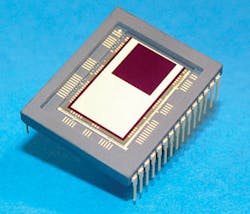
By coupling the unrivaled quantum efficiency performance of back-thinning with low read noise, the CCD97 complements the back-thinned CCD 60. The back-illuminated CCD 60 was the first CCD to offer sensitivity close to the theoretical maximum for a silicon imaging sensor, with quantum efficiency greater than 90% and read noise less than 1 electron, extending the scope of CCD sensor applications to include confocal microscopy, single-molecule imaging, and adaptive optics.
The CMOS counterpart to this CCD-based electron-multiplication technology is so-called Geiger-mode avalanche pixels. While still more experimental, these are similarly impressive. At a pixel size of about 30 µm, the devices are capable of detecting a single photon. However, further developments will be necessary to increase the fill factor in such devices from their current 5%.
Operated in the so-called Geiger mode, avalanche photodiodes can count single photons. In operation, each single-photon avalanche diode (SPAD) is a p-n junction biased above breakdown voltage by an excess voltage of a few volts. A primary carrier resulting from the absorption of a photon may generate an infinite number of secondary electron-hole pairs by impact ionization. Upon arrival of a photon, the breakdown current discharges the depletion region capacitance, reducing the voltage across the SPAD to its breakdown voltage. The near-infinite internal gain inherent in Geiger-mode operation requires no further amplification, and the pixel output can be routed directly outside the chip.
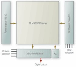
At the Swiss Federal Institute of Technology, a single 32 × 32 SPAD imager has been developed specifically for use in a 3-D camera (see Fig. 3). Based on the pulsed time-of-flight method, the sensor is implemented in standard CMOS technology and consists of an array of single photon avalanche diodes, capable of performing 1024 independent distance measurements.
MARTIN WÄNY is founder of Awaiba, Madeira, Portugal; www.awaiba.com.

null