Understanding camera performance specs
Camera Specs for Machine Vision Applications
Performance specifications and actual performance should be clearly understood when integrating sensors and cameras into vision systems.
By Andrew Wilson, Editor
Deciding on which camera suits any particular machine-vision application is complex. This is especially true when deciding on whether cameras based on CMOS image sensors can meet the needs of the application. A number of reasons make the choice of any particular camera complex, including partial, misleading, or difficult-to-compare specifications issued by manufacturers.
To compare specific cameras, information such as the quantum efficiency (QE), the dark noise, and saturation capacity of the sensor/camera combination must be known. From these measurements, maximum signal-to-noise ratio (S/N), absolute sensitivity, and dynamic range can be determined before deciding on what type of interface best fits the specific needs of the machine-vision application.
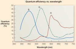
Quantum efficiency of both CCD and CMOS sensors is calculated as a ratio of the charge created by the device for a specific number of incoming photons. As the QE will change over different wavelengths, it is usually plotted as a function of wavelength. Generally, this reaches a maximum when green light of about 550 nm is present. This provides a measure of the sensitivity of the device. When implemented within a camera, the maximum QE of the camera should be less than that of the sensor, due to external optical and electronic effects.
The QE of the MT9T001, 1/2-in. CMOS image sensor from Micron Technology peaks at approximately 550 nm at a value of approximately 37% (see Fig. 1). In comparison, the KAF-3200, 2184 × 1510 CCD imager from Kodak Image Sensor Solutions is specified with a 70% QE at 550 nm. In choosing a camera for a particular application, camera QE performance is also provided. Unfortunately, this can sometimes be confusing. Soliton Technologies, for example, uses the MT9T001 in the design of its M211-CFW30, a FireWire area-scan camera. But rather than specify QE in percentages, this figure is presented as a “relative response,” which gives only a relative, not absolute, measurement of QE.
Dark noise and saturation capacity are also important parameters for camera designers. While dark noise measures the variation in the number of electrons that are thermally generated within the CCD or CMOS imager itself, saturation capacity describes the number of electrons that an individual pixel can store. While these parameters are generally not specified on camera manufacturers’ data sheets, they can be used with QE measurements to derive maximum S/N, absolute sensitivity, and the dynamic range of a camera.
Deriving details
The S/N can only be used as a rule of thumb when provided as the sole figure for camera performance. Certainly, an S/N of 20 dB may result in a camera with so much noise that the image is unusable for machine-vision applications, and one with a 60 dB ratio may appear to have very little noise. But here again, camera vendors can interpret and report these specification is different ways (see “Measuring the signal-to-noise ratio of digital cameras,” p. 42).
Possibly the easiest way for manufacturers to convince customers that one camera is better than another is to use this spec. And what better way to accomplish this than to use the theoretical S/N of the ADC used in the camera. In theory, using an 8-bit ADC, for example, should result in a maximum S/N of 8 bits or approximately 56 dB.
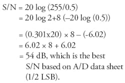
This formula comes from error simulation of linear vs step value in an ADC. Since a typical ADC is specified as the resolution or error at 1/2 LSB and 0.5 used as the noise value, the 8-bit S/N is calculated as
null
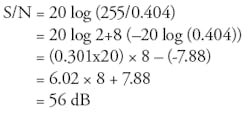
However, the theoretical error factor is 0.404 instead of 0.5 and from which the S/N is derived as
null
However, this is the S/N of the ADC and has nothing in common with the S/N of the camera. This is usually limited by the number of photons. In the case of the ADC, the dynamic range is usually specified. For example, a normal camera might have about 60-dB dynamic range and a S/N of 40 dB.
For a camera, the number of photons required to achieve saturation is the saturation capacity/QE. For a camera that requires 20,000 photons to reach saturation at a QE of 50% (0.5), the number of photons will be 40,000.
Since the noise is given as the SQRT (signal) = SQRT(40000) = 200, the S/N = 40000/200 = 200 = 46 dB or 7.6 bits. However, since the S/N of a camera is the number of electrons required for saturation divided by dark noise, a camera with 20,000 electrons full-well capacity and 15 electrons dark noise will yield a dynamic range of 20,000/15 = 1330 = 62.5 dB or 10.4 bits.
However, a camera’s S/N is not totally dependent on the S/N of the converter. The LightWise LW-5-S-1394 FireWire camera from Imaging Solutions Group (ISG), for example, uses Micron Technology’s 2592 × 1944 CMOS imager MT9P001. Despite the fact that the CMOS imager includes a 12-bit ADC, the S/N of the imager is specified as 38 dB. But the S/N of the camera is specified as “>38 dB.”
Rarely specified by any camera vendor, absolute sensitivity of a camera can be derived as a ratio between the dark noise and the QE of the camera. If, for example, the dark noise of a sensor is 50 electrons and the quantum efficiency of the imager is 50% at 550 nm, then the absolute sensitivity will be (50/(1/2)) or 100 photons. This is a measure of the minimum number of photons that can produce a minimum possible signal in the sensor or camera.
Often confused with S/N, the dynamic range of a camera is also expressed in decibels or number of bits. For sensors that behave in a linear fashion, the dynamic range is the ratio of the brightest unsaturated signal to the darkest possible signal detectable in the presence of noise. In the SI-1920HD MegaCamera from Silicon Imaging, for example, which uses a 1920 × 1080 CMOS imager, the dynamic range is 68 dB while the S/N is 52 dB at 0 dB gain. Since 68-dB dynamic range cannot be digitized with an 8-bit ADC, the SI-1920HD uses a 12-bit converter to digitize the signal from the sensor.
Impressive specifications
While comparing such measurements sounds relatively simple, in practice it is more difficult because of the lack of a standard way of comparing the cameras. In theory, camera vendors should produce datasheets on their products that test their cameras under a standard set of lighting conditions and produce specifications that reflect measured images generated from the camera. Yet in the worst case, camera vendors will not supply datasheets for their product that detail any such data. Other manufacturers, realizing that test equipment to perform such analyses is expensive are content to copy specifications such as sensitivity, S/N, and MTF data from the data sheet of the sensor vendor.
The European Machine Vision Association has begun its 1288 standard initiative to define a unified method to measure, compute, and present specification parameters for cameras and image sensors. Driven by a consortium of manufacturers including AWAIBA, Atmel, Basler, DALSA, PCO Imaging, Stemmer Imaging, and others, the aim of 1288 is to provide a standard way of allowing system integrators to compare cameras with a unified datasheet. To accomplish this, manufacturers such as Basler have developed automated camera test tools to provide standard results for their product lines.
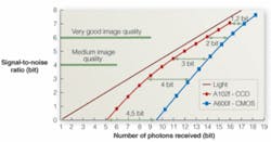
A number of different comparisons can be derived by plotting the S/N of the camera against the number of photons received. These charts can be used to compare the performance of CCD and CMOS-based cameras. For example, Basler’s A102f, a 1392 × 1040 CCD camera, is compared against the company’s A600f, a camera that incorporates Micron Technologies’ 656 x 491 MT9V403 CMOS imager (see Fig. 2).
As can be seen, the single chart at once relates the amount of light the camera is subjected to (as the number of photons received), the camera’s S/N, absolute sensitivity, and dynamic range. Interestingly, to obtain 6-bit S/N from these cameras requires 8000 (213) photons for the A102f CCD camera, while the CMOS-based A600f requires 33,000 (215) photons. At this point the CCD camera is four times (22) more sensitive than the CMOS camera. However, as the amount of light (number of photons) decreases, this distance increases, and at the point of saturation the CCD camera is 20 times more sensitive than the CMOS camera. Conversely, as the light increases, the CMOS camera reaches a higher S/N close to saturation because of its higher saturation capacity.
One class of devices that does not behave in a linear fashion was originally developed by Swiss Federal Institute of Electronics and Microtechnique and further developed by Photonfocus. Known as Linlog image sensors, these devices uses a linear response at low illumination levels and logarithmic compression at high intensities (see Fig. 3). Incorporated into the company’s range of progressive-scan CMOS cameras, the technology allows these cameras to exhibit a high input dynamic range, a feature especially attractive in applications such as laser triangulation where high light intensity would normally saturate a typical linear CCD or CMOS camera.
Spatial resolution
Determining the resolution of a camera can be one of the most important parameters. Many manufacturers specify the number of pixels used in the image sensor itself (such as 640 × 480). Unfortunately, without knowing the pixel pitch, one is unable to ascertain the theoretical resolution of the sensor.
Once the pixel pitch is calculated, the theoretical spatial resolution in line pairs (lp)/mm can be calculated. This spatial resolution provides a measure of the camera’s ability to distinguish two small structures or lines close together. To determine this, the camera must be tested with a bar chart and subjective measurements made. Unfortunately, this resolving power is not only dependent on the pixel size and dimensions of the image sensor. It is also dependent on lens resolution and the spatial noise related to the image sensor.
To test a camera’s resolving power, the theoretical limit can be calculated. Assuming that a dark line and bright line are resolved perfectly on neighboring pixels, the maximum resolution is given by R (max) = 1/(2p) lp/mm. Thus for a 10-μm image pixel, the maximum resolving power will be 50 lp/mm while for a 5-μm pixel, the resolving power will be 100 lp/mm. To obtain the maximum resolution possible, camera lens vendors must supply lenses with high optical resolution to provide the appropriate modulation transfer function for the small pixel sizes.
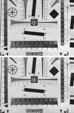
However, just as QE, S/N, and other parameters cannot be used solely to determine camera performance, neither can spatial resolution. In a comparison between an image taken with a Genie M640-1/3 from DALSA using a 1/3-in. Sony CCD sensor and a DALSA Genie HM640 using a DALSA-developed CMOS imager, pixel sizes and the lens used to image the test charts were the same, so it is very difficult to determine from spatial resolution alone the difference between the two cameras (see Fig. 4).
While the initial steps taken by Basler and others of the 1288 consortium are to be greatly praised, it may be awhile before complete specifications that system integrators can easily use become available. With such specifications, the choice of camera performance will no longer depend on the art of writing specifications and will allow rapid camera comparisons to be made.
Measuring the signal-to-noise ratio of digital cameras
Traditionally, the way to calculate the signal to noise ratio (S/N) of analog cameras is to measure both the signal and noise of the camera’s analog video signal using an oscilloscope or video S/N test equipment. This measurement, defined as
20 log (saturation signal/rms noise)dB where saturation signal = 100 IRE = 714 mV is not clearly defined for digital cameras.
Analog rms noise is defined at a specified uniform lighting, typically half that of the camera’s saturation level (50 IRE). This rms noise includes shot noise, which is proportional to the intensity of light falling on the imager used in the camera. To improve this S/N, filters are used to reject both high frequency and low frequency signals.
However, in digital cameras image data are generally not filtered, and, regardless of fixed pattern noise or multiframe random noise, overall noise appears in the black image. Thus, there is a clear relationship between overall noise and the dynamic range of the camera. However, because it is difficult to obtain rms noise for multiframe cameras, each manufacturer uses completely different methods to specify its camera’s S/N.
In the most extreme cases, this includes taking the dynamic range or S/N from the image-sensor manufacturer’s data sheet or using the resolution of the analog-to-digital converter (ADC) used in the camera. In digital cameras, for example, S/N is limited by the A/D resolution. For a camera that uses an 8-bit converter, this theoretical limit is 56 dB.
Imager noise can also affect the overall performance of digital cameras. This includes dark current noise, reset noise, shot noise, CCD surface noise, and output FET source follower noise. However, total camera noise must include both ADC quantization noise and circuit generated noise such as power supply switching noise.
To make these measurements, dark-image-noise-floor measurements can be used to compare the S/N of various cameras. Using the black image, shot noise can be ignored and black-level pixel uniformity maintained. This can be done by capturing black images with the camera lens closed and saving the data in raw data or bitmapped format.
To measure digital video camera noise characteristics, low-cost PC-based software such as Adobe Photoshop can be used to compare the S/N of various camera manufacturers and models. This is accurate and consistent for all digital cameras. Although the process is limited to 8-bit images, if the raw data are greater than 8 bits, the most significant 8 bits within the image are used providing reasonably accurate estimate of the original data.
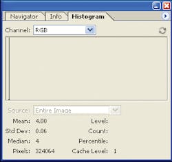
After saving the black video image in bitmap or raw data format, the histogram function in Photoshop will display the number of pixels with a specific brightness value (see figure). Ideally, every pixel in the image will have a black level value of zero. In practice, of course, this is not the case because it must avoid any negative values in overall temperature and gain range.
Using the “extended view” function of Photoshop histogram, it is then possible to select the entire field of view and measure the standard deviation. In a single-frame histogram, the rms noise and standard deviation is equal and can be applied to calculate the S/N of the camera:
S/N = 20 log (255/standard deviation) dB
Using this technique, system integrators can accurately determine the S/N of their CMOS- or CCD-based cameras.
Toshi Hori, president
GEViCAM
Milpitas, CA, USA
www.gevicam.com

