Multitechnology system checks PCBs
Automated optical inspection, x-ray imaging, infrared cameras, and acoustic microscopy are teamed in NDT system.
By Ian Nicholson and Winn Hardin, Contributing Editor
As the complexity, density, and cost of printed-circuit boards (PCBs) continues to escalate-particularly related to embedded electronics for medical and other real-time critical systems-so does the cost of reworking defective boards. Most finished electronics are checked with in-circuit testing (ICT) of functional blocks; however, inline inspection systems would locate defects before additional value is added to a defective product, thereby reducing repair and rework costs.
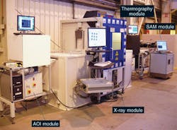
High-value microprocessors, FPGAs, and DSPs are forcing some electronics manufacturers to move traditionally offline nondestructive-testing (NDT) systems-such as x-ray, thermography, and acoustic microscopy-to their production lines to achieve 100% inspection. It was with this trend firmly in mind that several small-to-medium-enterprise (SME) European companies and two European research institutions-Kaunus University of Technology (KTU) and Fraunhofer-Institut für Produktionstechnik und Automatisierung IPA-partnered to develop the Microscan PCB inspection system, which combines the three most common offline inspection technologies with automated optical inspection to provide 100% inline inspection of populated PCBs (see Fig. 1).
The various inspection systems were developed to work separately, but were also designed to work with common data and material handling interfaces so that end users could either pick and choose among the systems depending on the PCB inspection requirements or use all four systems. As part of the EU Framework 6 CRAFT-funded program, SMEs were chosen from across Europe with expertise in various NDT technologies. X-Tek builds microfocus x-ray systems for the inspection of all components including PCB assemblies, LOT develops thermal-imaging and examination systems, Machine Vision Products develops AOI systems, and Ultrasound Sciences develops scanning acoustic microscopes (SAMs) to examine PCB components.
Microtel and Beta Electronics are leading manufacturers of PCBs and Goodrich Engine Control Systems is an end user that assisted the project by providing PCBs for checking and general integration requirements and guidance. Also, this project brought together RTD centers in NDT, acoustic inspection (KTU), and x-ray image-processing software development (IPA).
Targeting 100% Defects
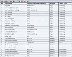
Although every electronics-manufacturing line will have its own unique challenges and quality-control requirements, one of the first efforts as part of development of the Microscan electronics inspection system was to get all partners to agree on the most common defects and then build a number of prototype systems that worked on common standards. The Microscan group developed a “top 24” inspection wish list of the most common defects on electronic boards, starting with dry joints, moving through solder shorts and bridges more common to the new generation of lead-free solders, to ball-grid -array (BGA) inspection, and concluding with missing or misaligned components (see table).
The defect list was collated with the most appropriate Microscan inspection systems and prioritized based on the cost to rework the board. A missing capacitor can be considered less of a problem than a bridged lead on an expensive BGA microprocessor, for example. Electronic board manufacturers Beta Electronics and Microtel manufactured and supplied boards with samples of specific defects, as well as ‘golden parts’ for training the systems.
System integrators then agreed to use IPC’s Surface Mount Equipment Manufacturers Association (SMEMA) standard for electronic boards material-handling systems (such as electronic interface, physical dimensions, permissible conveyor height, and PCB edge clearance) to enable the systems to be connected to each other and to other PCB manufacturing equipment. The group also developed a unified software framework executed on each inspection prototype host PC to monitor machines connected upstream and downstream.
The systems are designed to operate in pull configurations for easy integration with most standard electronics manufacturing lines. (In pull systems the board will not leave a workcell until called by the next downstream node, eliminating the need for a separate cell controller for each node on the production line.) A pass or failed component is indicated by an alarm, an on-screen flag, and an entry saved to a results file local to each prototype. In addition each inspection prototype PC has the capability to be networked via 10/100 Ethernet, thus allowing a remote operator to interrogate all the prototype results files for statistical analysis from a single PC connected to the network.
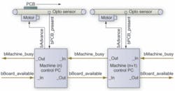
As part of the SMEMA standardization effort, TWI developed a generic SMEMA communications and control board to connect each PC host to the SMEMA communications interface network and to control each inspection module’s conveyor. The SMEMA board was initially developed with the AOI system as a testbed and was later rolled out to the x-ray, ultrasound, and thermal-imaging inspection systems. The SMEMA communications interface is a simple two-signal communications method comprising Board Available and Machine Ready signals (www.ipc.org/html/IPC-SMEMA-9851.pdf) and is bus independent.
Starting with AOI
Microscan’s AOI system was designed to inspect boards after any of the three main stages of manufacture-solder paste printing, component placement, reflow oven-and provide a test bed for image-processing algorithms that would be reused on the x-ray and SAM inspection systems; the IR system has its own software. At each step, AOI systems can locate defects and designate boards for rework before additional value is added.
The AOI system was created with an ambient-light limiting enclosure fed by an edge belt/side rail conveyor built by Central Conveyors. The conveyor was custom-built according to the Microscan group’s request and was developed in such a way that it could easily be mechanically and electrically incorporated in all the inspection prototypes. As specified by SMEMA, a moveable back rail allows the edge conveyor to accommodate PCBs of varying sizes and restricts transverse motion of the PCB with respect to the conveyor motion. A servo drive system offers guaranteed mechanical stops to ensure that the board’s actual position is always within a 0.2-mm stopping tolerance. An onboard controller facilitates simple start/stop control of the conveyor and board detection.
During inspection, the PCB board enters the conveyor, and an IR optosensor signal is carried across a USB 1208FS data-acquisition module to the SMEMA software running on the PC. Initially, the sensor was located too far away from the conveyor, and reflections from metal components on the edge of the PCB could cause the conveyor to stop before or after the optimal position for inspection. Placing the sensor closer eliminated this problem.
This USB I/O controller is used in all the prototypes apart from the SAM prototype, which uses a proprietary I/O controller. However, the group agreed to standardize the inputs and outputs by manufacturing a control PCB. The board incorporated opto isolators and relays and was designed with an area of the board that matched the footprint of the USB I/O controller, allowing the USB I/O controller to be piggy backed on back of the board, or as in the case of the SAM, a specially designed PCB the same shape as the USB I/O controller but with a connector that accepted a ribbon cable connection from the SAM I/O port, which is part of the proprietary electronics designed by USL. With four different main partners developing the prototypes, all working to the same specification, this circuit design reduced integration issues among the different systems through use of common signals and connectors.
In consultation with MVP, the AOI specialists at TWI developed the AOI software in MS Visual Studio.NET C++, placing emphasis on the robustness of the algorithms. Specifically, algorithms were developed for registering the sample photo from the camera to the original and image subtraction. Camera controls and image-acquisition source code were packaged along with the Hitachi Kokusai Electric KP-F120 CCD camera and Nexeon CL PCI Camera Link frame grabber from dPict Imaging.
Camera Link provides the connection between camera and frame grabber, while a dozen, 3.3-V bulbs on the sides of the conveyor provide effective illumination. The bulbs were located out of direct view and below the camera to avoid shadows and provide equal illumination of the components.
In the PC host’s memory, the acquired image is preprocessed, using geometric pattern search, to locate local PCB fiducial marks for each operator set region of interest. The acquired image is then registered to a stored ‘golden image’ of a defect-free PCB board, and the acquired pixel values are subtracted from the original image. The residual bright spots are compared against a threshold determined by histogram of the defect-free board. The remaining “bright spots” are then grouped to assist in defect analysis and filter out spurious reflections that would produce false errors. The final pass/fail is then stored on the local PC hard drive, but in a production environment, a SMEMA 9851 pass/fail signal would be sent to upstream and downstream nodes on the production line to continue production (see Fig. 2)
x-ray Builds on AOI
AOI cannot image hidden features such as solder pads under BGAs. Therefore, an x-ray system was developed to build on the lessons of the AOI system.
Developed by X-Tek Systems, the x-ray inspection is controlled by a local PC running InspectX software for source and detector controller. A microfocus electron gun housed in a vacuum chamber is aimed at a tungsten foil target to produce x-rays of varying energies between 40 to 160 kV. A digital camera is optically coupled to a phosphor screen to produce 758 × 580-pixel, 12-bit monochromatic images of an x-ray radiograph. A nominal stand of distance between source and PCB of 60 mm provides magnification up to 1200X.
The PCB enters through a lead-lined tunnel, and an optosensor triggers the InspectX system control software. A five-axis manipulator within the chamber grabs the PCB and orients it to image a particular component. The acquired x-ray image is noisy, so a 5 × 5 moving rank filter cleans up the image. The image is segmented into white and black (binary) pixels based on a local thresholds set by running histograms on the golden part image; global thresholds produced inaccurate binary visualizations because of changing background pixel values. Missing solder, cracked, bridged, or whiskered solder balls are readily identifiable in the final binary image (see Fig. 3).
The x-ray system initially included a PCB manipulation system that would tilt the board in relation to the source and allow the x-ray system to image the board from multiple angles. Fraunhofer IPA produced algorithms for looking at defects specifically for poor BGA ball wetting. The manipulator in the x-ray machine tilts the PCB at angles up to 60˚ to reveal the shape of the balls. If viewing just top down-not an oblique angle view-typically poor wetting cannot be imaged. However, application of the poor wetting detection algorithms depended very much on the type of PCB. This is due to practical restrictions in positioning the board relative to the x-ray source and detector. Increasing the angle of the PCB too much results in collision with either the x-ray source or conveyor.
InspectX enables the x-ray inspection module to be fully automated using a Visual Basic for Applications (VBA) script. After development of the AOI algorithms, it was straightforward to rewrite them in a VBA script and incorporate them into the InspectX to detect bridging, twisted BGAs, and missing BGA defects. These types of defects can be imaged/detected without repositioning the board at an angle.
SAM Delamination
Shorts and delamination of PCB boards and IC packages were among the most important targets for the IR imaging system. In the initial prototype a FLIR Systems Phoenix 3-5-µm thermal camera was placed inside an enclosure built to filter out ambient light and accommodate the SMEMA conveyor.
Two 500-W pulsed flashlamp illuminators were incorporated inside the enclosure to heat the PCB using a single flash and produce an active IR image. While initial experiments showed that active illumination could detect delamination of both PCB board layers and IC packages, better data could be provided by the SAM system. This allowed the IR system to locate shorts with great clarity in a simpler passive imaging mode.
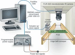
To operate the IR system in passive mode, the flashlamps were replaced with a spring-loaded linear actuator that powered critical circuits on the PCB. In addition, the IR camera was replaced with a FLIR A20 IR camera that can indicate the temperature of objects instead of producing a thermal image and is better suited to process control and monitoring environment. Spare I/O on the USB 1208 module was used to control the actuator, using system software developed in VisualBasic script (see Fig. 4). Images from the A20 are passed over FireWire connection to a 1394 board in the PC, and FLIR’s ThermCam Researcher software conducts threshold convolutions to locate areas indicative of electrical shorts (see Fig. 5).
The final SAM system raster scans an ultrasonic probe above each component to be inspected. In SAM systems water provides the medium whereby ultrasonic waves can be transmitted from the probe into the component under inspection. Unlike existing offline SAM systems, the prototype uses a column of sprayed (deionized) water instead of than submersing the PCB in water to enable acoustic imaging. This proprietary method reduces the chances of water being trapped between components and the PCB, and facilitated easier integration with the conveyor.
The SAM prototype software comprises two applications running in parallel and in the same subfolder on the SAM PC. One application was written by USL and controls the operation of the SAM hardware. The other application was developed by TWI with input from KTU and is responsible for determining if an acquired image represents a pass or failed component. TTL logic level signals between the SAM I/O (controlled by the USL application) and a USB 1208 I/O module (controlled by the TWI application) flag and synchronize the programs, while text files are used to transfer parameters.
The partners adopted this approach because the SAM control software is complex and did not have the inbuilt scripting facilities like those provided for the InspectX and ThermCam Researcher thermography software. Sample SAM images show an example of a good and a bad delaminated BGA component. The differences are quite visible (lighter areas indicate delamination) and are easily detectable and sentenced with the registration and subtraction algorithms originally developed for the AOI system.
Ian Nicholson is principal project scientist at TWI Technology Centre, Port Talbot, UK; www.twi.co.uk.


