Speeding Up the Bus
Designers remain wary of the latest PCI Express developments
Ever since the PCI Express interface replaced PCI and PCI-X designs in PC-based computers, most frame-grabber vendors have adopted the standard as the architecture of choice for their current and next-generation products. But just as higher-speed cameras require vendors to re-evaluate point-to-point interfaces such as the Camera Link standard, so too must vendors of PCs and add-in cards increase the speed of these interfaces.
In 2007, members of PCI-SIG, the industry organization chartered to develop and manage the PCI standard, introduced two new standards that increase the speed of PCI Express while adding (and removing) some of the features of the original specification. In the original specification now adopted by PC and frame-grabber vendors, data are transferred from the frame grabber to the host computer using pairs of LVDS transceivers that can be scaled by adding signal pairs, resulting in x1, x4, x8, and x16 lane widths. In the most commonly available low-cost frame grabbers, x1 interfaces are used. The transceivers on these boards are capable of transferring data in each direction at speeds as fast as lane carries 250 Gbits/s in each direction.
However, because PCI Express architecture encodes 8-bit data bytes into 10-bit transmission characters using the 8b/10b protocol, the effective bidirectional bandwidth is 80% of this, or a maximum unidirectional bandwidth of 250 Mbytes/s. This results in a number of different transfer rates depending upon which configuration is chosen. Although a maximum 4 Gbytes/s for a x16 configuration was very useful for graphics-card vendors, some consumer motherboards only support the PCI Express bus for graphics cards, and, as such, x16 frame-grabber configurations are not generally offered by frame-grabber vendors.
Members of PCI-SIG also realized the data-transfer limitations of the bus and have proposed amendments to the existing standard that will dramatically increase these speeds. In January 2007, for example, PCI-SIG released PCI Express 2.0, which doubles the LVDS interconnect bit rate from 2.5 to 5 Gbits/s to support high-bandwidth applications. At the same time, the committee renamed the transfer rate as 5GTransfers per second (5GT/s) to alleviate the common misconception that this data rate was actually achievable with 8b/10b encoding.
Faster and faster
According to the committee, PCI Express 2.0 extends the data rate to 5GT/s (read 5 Gbits/s) in a manner compatible with all existing PCIe 1.1 products currently supporting 2.5GT/s (read 2.5 Gbits/s) signaling. According to PCI-SIG, the key benefit of PCIe 2.0 is faster signaling, effectively increasing the aggregate bandwidth of a 16-lane link to approximately 16 Gbytes/s (but a peak unidirectional bandwidth of 8 Gbytes/s).
Effectively, this doubles the bandwidth of the existing standard. In addition to faster signaling, PCI-SIG working groups added several protocol layer improvements including dynamic link speed management, link bandwidth notification, access control services allows for optional controls to manage peer-to-peer transactions and function-level reset.
Even before many engineers had had time to digest this new standard, in August 2007 PCI-SIG upped the ante on the standard by introducing PCI Express 3.0, which increases the LVDS transceiver bit rate to 8GT/s (read 8 Gbits/s). According to Rick Merritt writing in EETimes, the decision to settle on 8 Gbits/s ends a lively debate that has stretched over several months as to whether 8 or 10 Gbits/s was the right step for the 3.0 version of the standard.
While some engineers argued that higher throughput was needed, ultimately a concern over cost and compatibility issues drove engineers to decide on a more modest step forward. “Experts in the PCIe Electrical Workgroup analyzed both 10GT/s and 8GT/s as target bit rates for the next generation of PCIe architecture and, after careful consideration of several factors, including power, implementation complexity, and silicon area, recommended 8GT/s,” said Al Yanes, PCI-SIG chairman.
Interestingly, to double the bandwidth of PCI Express-based systems that will use these transceivers, the standards committee has abandoned the requirement for the 8b/10b encoding scheme supported in prior versions of PCIe architecture, which imposed a 20% overhead on the raw bit rate. Thus, two pairs of transceivers operating at 8 Gbits/s will result in a 1-Gbyte/s peak unidirectional data-transfer rate in a single x1 PCI Express 3.0 configuration, making the standard effectively twice as fast as Version 2.0 and four times faster than the current standard.
According to PCI-SIG, the PCIe 3.0 specification will feature enhanced signaling and data integrity, including transmitter and receiver equalization, PLL improvements, clock data recovery, and channel enhancements for currently supported topologies. The final PCIe 3.0 specifications, including form factor specification updates, may be available by late 2009 and could be seen in products starting in 2010.
Building a frame grabber
“The PCI Express specification maintained by the PCI-SIG mandates that every PCI Express device use physical, data link, and transaction protocol layers,” says Alex Goldhammer, technical marketing manager with Xilinx.” A single PCI endpoint can be built using a single- or two-chip solution. For example, a Xilinx Spartan FPGA can be used with soft-IP for the data-link and transaction layers in conjunction with a commercially available discrete PCI Express PHY. “This option is best suited for x1 lane applications such as bus controllers and data-acquisition cards,” he says. Such discrete PHY devices are available from a number of vendors including NXP Semiconductors.
Alternatively, a single-chip device such as the Virtex-5 LXT or SXT FPGA with integrated PCI Express data link and transaction protocol and built-in PHY can be used. This is best suited for communications or frame-grabber boards that require higher performance of x8 and x4 systems (see “PCI Express interface transfers image data,” p. 48).
While Xilinx is yet to announce such a part to support the PCI Express 2.0 standard, its major competitor, Altera has already endorsed the standard with its Stratix II GX FPGAs. With up to 20 low-power transceivers, the device delivers 100 Gbits/s of aggregate bandwidth on backplanes up to 1 m in length and up to 80 Gbits/s on 15 m of copper cable. Using the Stratix II GX-based PLDA Xpress GXII prototyping board, the company also demonstrated data transmission over 98 ft of PCI Express cable at the PCIe 1.1 rate of 2.5 Gbits/s. Although such devices are becoming available, their cost is prohibitive for many frame-grabber designers at present. “Only Altera supports PCI Express 2.0, but the cost of the PLDA IP is $40,000--a bit out of the ballpark at present,” says Chuck Petersen, president of Epix.
“All of the Virtex-5 “T” family of FPGAs have built-in PCI Express 1.1 blocks and integrated transceivers. By having the PCI Express data link layer and transaction layers built in to the silicon, very little of the FPGA fabric is used. Further, because the block is built in to the silicon, there is no licensing cost. In short, the built-in block gives the FPGA user the benefits of an application-specific processor with the benefits of an FPGA,” says Goldhammer.
Not an easy task
But PCI-Express development is not for the weak-hearted designer. “It is an expensive and complex enterprise,” says Avner Butnaru, CEO and chairman of Bitflow. “Most frame-grabber designers implement PCI Express in a large FPGA, since a large amount of real estate is required just for the PCI Express implementation. Indeed, nearly every designer purchases the PCI Express core, which is not inexpensive. To support PCI Express, an FPGA should have the serial-deserializers (SERDESs) on-chip, which automatically increases the price of the FPGA by about 30%. Testing and debugging such devices is also not an easy task, since many PCI Express cores are encoded and must be treated as black boxes. And with PCI Express signals in the gigahertz range, debugging poses a significant task.”
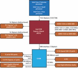
In October 2007, Intel and AMD released chipsets that support PCIe 2.0. For its part, Intel’s first chipset to support the standard, the X38, is designed for use with its Core 2 Duo and Core 2 and Quad processor and consists of a 82X38 memory controller hub host bridge and ICH9 I/O controller hub. Unfortunately, those expecting a chipset capable of supporting a number of PCIe 2.0 configurations may be disappointed.
Like other chipsets before them, Intel is chasing the largest market with its X38. So while the 82X38 can support two x 16 lanes of the PCIe standard, the older ICH9 only supports the slower 1.1 interface standard making the chipset a firm target for the games market. Despite this, a number of motherboard vendors including Universal Abit, Asus Computer, and Gigabyte Technology have released motherboards based on the chipset.
“While higher speeds are desirable to reduce the cost of a multilane board, processing limitations of the PC are the real limiting factor of these higher bandwidths,” says Joseph Sgro, CEO of Alacron. “The biggest benefit will be to applications that need to switch data without actually processing it, for example, in networking applications. Graphics processors also can use this bandwidth because generated images are displayed and discarded. However, typical frame grabbers cannot use this additional bandwidth effectively. For frame-grabber companies, higher data rates are not necessarily required since the PC just can not handle the extra data. Of course, logic is seldom present in product marketing, so we will most likely have to develop products that support these new data rates in the future,” he says.

Most of the chip sets from Intel and AMD provide either one or two x16 ports for graphics cards, which could be used by frame grabbers, on the North Bridge (see figure). These ports provide the ability to transfer images into PC memory at a high rate. “But even if image data are transferred at the full 4-Gbytes/s data rate, the processor has to read the data at 4 Gbytes/s and write it back to memory at 4 Gbytes/s,” says Sgro. “This uses a 12-Gbyte/s memory bandwidth so the memory system is more than half loaded (21 Gbytes/s), and the processors bus is 80% loaded using Extreme, Quad, or Duo processors or half-loaded using Xeon processors.
Although the South Bridge (ICH8 and 9) provides additional PCIe support, no additional speed up can be achieved by connecting to the South Bridge. Indeed, it is not clear that x16 or higher-speed PCI Express bus protocols will drive a large segment of the frame-grabber or camera manufacturer market, since most applications are either compute or storage bound for the foreseeable future.”
“Assuming that the bottleneck with processing and storing the data is removed,” says Andrew Buglass, product manager of Active Silicon, “the current x4 interface can just about cope with the maximum speed of a Full Camera Link (v1.1) camera, which is a theoretical 680 Mbytes/s. If the Camera Link interface speed is increased (see Vision Systems Design, October 2007, p. 79), then a x8 PCI Express interface may not be able to cope with the data rates.” Worse, x16 PCIe boards will be more expensive to make.
PCI Express interface transfers image data
More than three years ago, Vision Systems Design predicted that because of the flexibility offered by the scalable serial point-to-point architecture of the PCI Express (PCIe) interface, it might be adopted by camera vendors as the next high-speed digital interface. However, up until Vision 2007 in Stuttgart, Germany, held in November, no camera vendors had adopted the standard. But at the show, Point Grey Research exhibited two technology demonstrations of prototype cameras that used the PCI Express 1.1 standard to interface two very different cameras to a PCIe digital interface housed in a PC.
In the design of its first camera, Point Grey engineers chose to build on their existing Grasshopper camera platform. The Grasshopper couples the new ICX625 5-Mpixel Super HAD CCD from Sony with a dual-channel, 14-bit, 65-MHz analog front end (AFE) from Analog Devices, used for sensor timing and control.
A new physical layer and FPGA, however, were required for the PCIe interface to work. “The Virtex-5 LX FPGA from Xilinx implements the logical and transport layers of the PCI Express 1.1 interface,” says Vladimir Tucakov, director at Point Grey Research, “while the x1 physical interface is performed by an XIO1100 dedicated PHY from Texas Instruments (TI). “Although a Virtex-5 LXT or SXT Series FPGA could have been used to implement transaction layer, data link layer, and physical layer functions,” says Tucakov, “this solution would have been more expensive. The camera was intended solely as a technology demonstration, so we chose to minimize extra costs by using the Virtex-5 LX.”
To interface the PCI Express camera to the host PC’s PCI Express bus, an EEX1 PCIe host adapter card from Magma was used. Using a 3m PCI Express-approved cable from Molex, the camera was demonstrated streaming 1920 × 1080-pixel 24-bit RGB images at 22 frames/s from the dual-tap CCD imager to the host PC, for a total data rate of 136 Mbytes/s. Under the PCI Express 1.1 specification, cable lengths up to 7 m are allowed.
Equally if not more impressive was a demonstration of a lightfield camera with PCI Express interface, the ProFUSION 25, which was developed by Point Grey’s Japanese distributor, ViewPLUS. “With lightfield cameras, several images of a scene are taken from physically offset viewpoints,” says Tucakov. “This gives us directional information about the light hitting the camera in a plane—the “light field”—rather than just a single point, such as a traditional lens. The applications of light fields are still emerging. However, examples are the ability to select the depth-of-field of a photograph after it is taken, or the ability to render novel 3-D views of the scene without explicitly reconstructing a 3-D model of the image.”
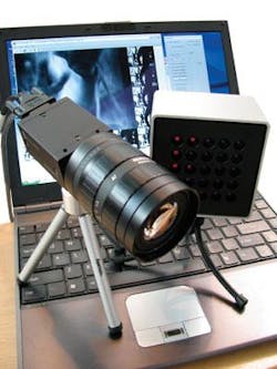
These types of cameras can be designed in different ways, namely with a very large imager using multiple lens systems such as those recently developed by Adobe Systems or by using multiple cameras, each with different lens elements. While the recently announced lightfield camera from Adobe uses a 16-Mpixel CCD imager and a hexagonal array of lenses (see “New Light Field Camera Designs,” Todor G. Georgiev: www.tgeorgiev.net/LightFieldCamera.pdf), the ProFUSION 25 uses 25 VGA sensors, each with separate micro lenses in a 5 x 5 grid (see figure).
“By using low-cost MT9V022 wide-VGA CMOS sensors from Micron Technology, we have reduced the cost of such camera systems,” says Tucakov. “At the same time, the use of the PCI Express 1.1 interface allows the camera to transfer 640 × 480 images from all 25 imagers directly to the host computer’s main memory at rates as fast as 25 frames/s, for a total data rate of more than 192 Mbytes/s.”