Novel Niches
Andrew Wilson, Editor
More than 40 vendors supply a variety of imaging sensors to camera manufacturers using charge-coupled device (CCD), charge-injection device (CID), and complementary metal oxide semiconductor (CMOS) technology. While most of these devices operate in the visible spectrum, a number of vendors also offer devices with enhanced UV and IR response, allowing camera manufacturers to develop products with a wider spectral bandwidth.

While camera vendors targeting the machine-vision industry may use just a handful of interline CCD and CMOS sensors from even fewer vendors—most noticeably Aptina Imaging, Kodak, and Sony—specialized CCD and CMOS vendors are targeting both high-volume consumer markets and smaller niche markets such as astronomy with their devices. While much has been written about the differences in architectures between CCD and CMOS image sensors, system developers are perhaps more interested in how the devices lend themselves to particular imaging applications.
Different architectures
CCD sensors can be fabricated in a number of different ways, each of which presents the camera developer with various price/performance tradeoffs. The most common types of these devices include full-frame imagers, frame transfer, and interline transfer devices. In full-frame imagers, all of the silicon area is devoted to image capture; therefore, these image sensors have 100% fill factor. Although these devices exhibit high quantum efficiency, a shutter is required to prevent image smearing since the collected charge is shifted sequentially across the array during image readout.
With front-illuminated CCDs, the photosensitive area of the imager is in front of the silicon substrate and light is reflected and absorbed there, which limits the quantum efficiency in the visible region and lowers UV response. To overcome this, some CCD and CMOS imager vendors have developed novel ways to increase the sensitivity of their full-frame imagers. Kodak, for example, uses a transparent gate in the design of its KAF-1001, a 1024 × 1024, two-phase, 5-frames/s full-frame imager that the company claims increases the spectral response by 50% over the sensor’s visible wavelength.
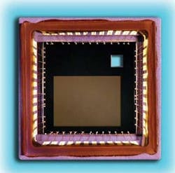
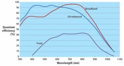
To increase this sensitivity further, a process called back thinning allows light to enter from the rear of the silicon substrate, eliminating absorption loss and at the same time increasing the quantum efficiency and the spectral range of the imager. The CCD 3041 from Fairchild Imaging, for example, is a 2k × 2k full-frame image sensor designed for scientific, space, and medical applications that features a pixel pitch of 15 µm and a 100% fill factor. Because many system developers required the extra sensitivity obtained by back thinning, the company offers the device in both front-side illuminated and back-thinned versions. The result of such back thinning nearly doubles the quantum efficiency of the device over the entire visible spectrum (see Fig. 1).
Increased sensitivity
While full-frame imagers use all the silicon area to capture photons, the requirement of an electromechanical or optical shutter adds cost to any systems that incorporate them. Furthermore, while the device is shuttered, no images can be captured. To alleviate this problem, frame transfer devices can be used. These devices use two image arrays—one exposed and the other shielded—to perform image capture. As light falls onto the photosensitive region, it is transferred to a storage array and then a readout register that transfers the image off-chip.
e2v uses this technology in its CCD201, a 1024 × 1024-pixel, two-phase CCD that operates at 15 frames/s and a fill factor of 100%. To increase quantum efficiency, the device is also back thinned. Designed to operate in conditions of low illumination, the CCD first converts photons to charge in the image area during the integration time period, then transfers this charge through the image and store sections into a readout register. Following transfer through this readout register, collected charge is then multiplied in the gain register before conversion to a voltage by an output amplifier.
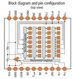
In machine-vision systems, where images must be captured rapidly, interline CCDs are most often used. In these devices, the charge transfer regions are incorporated onto the same silicon as the photosensitive area. Every other vertical column of the image sensor is masked with an image storage register and only a single pixel shift is required to transfer the image from the photosensitive areas to the vertical registers. Charge can then be clocked from the device at relatively high speeds. Although this results in an increased data rate, the fill factor and quantum efficiency of the devices is reduced since the image area is partially covered with data registers (see Fig. 2).
This method has been widely adopted by a number of companies including Sony in its range of interline transfer devices. Sony’s ICX205AL, for example, is a 1392 × 1024-pixel imager that allows image data to be read out from the device at a number of different frame rates. In progressive-scan mode, all the pixel data are output in noninterlace format in 1/7.5 s, making this mode suitable for high-resolution imaging. To increase this data rate, fewer pixels are read out from the imager, increasing the data rate to 1/30 s but reducing the vertical resolution by a factor of four.
CMOS devices
While many camera vendors use CCDs in their machine-vision cameras, others have tied their chariots to CMOS workhorses, most notably those from Aptina Imaging. Unlike CCD imagers, CMOS devices are based on active-pixel arrays, where each pixel site contains an individual photo-site and readout electronics. Because of this, the fill factor can never reach 100%. Although the performance characteristics of these devices are generally lower than CCD imagers, the integration of image sensor and readout electronics onto a single device results in a lower cost and simpler camera designs.
Despite being initially marketed as low-cost CCD replacements promising on-board processing capability, CCD-like performance, and lower power, the market for CMOS imagers has, up until now, remained in high-volume applications such as mobile phones. Perhaps the main reason has been that, despite all of the marketing hype, the image quality of CMOS imagers still, in most cases, remains far less than their CCD counterparts.
Slowly, however, the perception of these devices is changing with companies such as DALSA producing CMOS imagers and cameras that boast similar imaging performance to CCD-based cameras (see “Understanding camera performance specs,” Vision Systems Design, July 2007). To paraphrase Winston Churchill, while the battle of CCD vs. CMOS architectures may be over, the battle for niche imaging markets is about to begin.
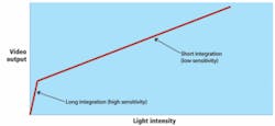
In many cases, such as high-speed and low-light-level imaging or where region-of-interest (ROI) image capture is required, CMOS-imager-based cameras have found strong market niches. In the design of its FireWire-based LW-WVGA-G-1394 camera, for example, Imaging Solutions Group has used an Aptina Imaging MT9V022—a 752 × 480 CMOS imager with 6 × 6-µm pixels that can run at 60 frames/s and faster in ROI mode. The MT9V022 pixel response can be configured for either linear light response with approximately 55 dB of dynamic range or for high-dynamic-range response with as much as 100 dB of dynamic range by controlling the slopes of a piecewise, linear pixel response (see Fig. 3).
Low light, high speed
While many companies attempted to boost the performance specifications of their CMOS imagers, others offered specialized devices that leverage the advantages of CMOS imagers for low-light-level and high-speed imaging applications. One of the most important developments in this area was the logarithmic image sensor that allows the sensor to exhibit a linear response at low illumination levels and logarithmic compression at high intensities.
Currently, Aptina Imaging, Cypress Semiconductor, and Photonfocus all offer devices that use this or similar technology to allow cameras based around these devices to exhibit a dynamic range of approximately 120 dB, a feature attractive in applications such as laser scanning where high light intensity could saturate CCD-based cameras.
Building on these developments, Photonfocus has recently announced its third-generation CMOS imager, the A1312, a 1312 × 1082 imager with an 8-µm square pixel size and four taps that allow the device to run at 120 frames/s. Initially, says Marcel Krist, Photonfocus’s newly appointed CEO, the device will not be offered with the company’s LinLog capability.
Instead, the company plans to develop a low-cost CMOS Camera Link camera based around the device to compete in the high-speed camera market. This will be followed by an IR enhanced version of the imager and a Bayer-based color version of the sensor and camera. Next year, the company will introduce a LinLog version of the camera that will allow 16 regions of interest (ROIs) from the camera to be processed in separate windows.
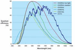
To evaluate the performance of initial samples of the A1312, Photonfocus called upon AEON Verlag & Studio. Data generated by AEON shows that the quantum efficiency of the new device compares favorably with CCD imagers with the A1312 boasting greater than 50% quantum efficiency at approximately 700 nm (see Fig. 4). Even when compared with interline CCDs from Sony this quantum efficiency response is impressive.
To improve the quantum efficiency further in CMOS imagers, researchers at the Rutherford Appleton Laboratory are developing CMOS Active Pixel Sensors (APS) that rely on adapting the back-thinning and rear-illumination techniques first developed for CCD sensors. In the development of a 4k × 3k-pixel sensor for space science applications, researchers found that at extreme ultraviolet (EUV) wavelengths, the absorption depth in silicon is so shallow that the oxide layers on front-illuminated CMOS sensors absorb the photons before they reach the photodiodes. To overcome this, wafer samples of the APS imagers were thinned by e2v to obtain good sensitivity at EUV wavelengths.
Interestingly, the move toward greater sensitivity in such CMOS imagers has been coupled with on-chip programmability. In automotive applications, for example, both STMicroelectronics and Aptina have recently introduced two devices targeted at vision-based driver awareness. STMicroelectronics VL5510 sensor has a 1024 × 512-pixel format, programmable output image size, and frame rate of up to 34 frames/s; the sensor also features 10 programmable knee points to allow the pixel response to be tuned for specific applications. Taking this concept further, Aptina has developed a complete system-on-a-chip, the MT9V126, which incorporates an on-chip imager and is claimed to eliminate the need for a DSP and an FPGA.
To meet the demand of niche imaging applications, semiconductor vendors now offer an array of different technologies ranging from multitap area-array imagers to novel time-delay integration (TDI) CCD and CMOS imagers for machine-vision and automotive applications. In the future, further developments in both CCD and CMOS imager architectures will lead to more sensitive, wider-spectrum devices that may encompass UV, visible, and IR applications. Coupled with on-chip and region-of-interest (ROI) processing, this will lead to a flurry of smart cameras and embedded imaging systems with more functionality and lower price/performance.
Company Info
AEON Verlag & Studio
Hanau, Germany
www.heurisko.de
Aptina Imaging, San Jose, CA, USA
www.aptina.com
Cypress Semiconductor
San Jose, CA, USA
www.cypress.com
DALSA, Waterloo, ON, Canada
www.dalsa.com
e2v, Chelmsford, UK
www.e2v.com
Fairchild Imaging
Milpitas, CA, USA
www.fairchildimaging.com
Imaging Solutions Group
Fairport, NY, USA
www.isgchips.com
Kodak, Rochester, NY, USA
www.kodak.com
Photonfocus, Lachen, Switzerland
www.photonfocus.com
Rutherford Appleton Laboratory, Didcot, UK
www.sstd.rl.ac.uk
Sony, Tokyo, Japan
www.sony.com
STMicroelectronics
Geneva, Switzerland
www.st.com