Into the UV

Using ultraviolet lenses in machine-vision applications reveals finer object details
Five years ago, York Winter, a researcher at Munich University and the Max-Planck-Research Centre for Ornithology, discovered that Central and South American bats that live on the nectar from flowers can see UV light. Lacking cone pigments in their eyes, the flower bats capture UV light with the rhodopsin or visual purple receptors of their rod pigments. The bats use their rod receptor cells to capture UV photons in these photoreceptors to perceive light radiation over the 310–600-nm spectrum. According to Winter, the bats need UV vision because the flowers they visit at night are characterized by a strong reflection of the UV spectrum.
Although human beings have lost their ability to visualize UV images, using shorter-than-visible radiation wavelengths has applications in industries such as semiconductor fabrication and inspection, glass, and high-resolution parts inspection. Unlike the evolutionary elegance employed in the bats’ visual systems, today’s machine vision systems that use the UV spectrum must be based on more basic products that involve off-the-shelf light sources, lenses, and CCD- or CMOS-based cameras.
Cut it up
Like many parts of the electromagnetic spectrum, the UV spectrum can be subdivided in several ways. As part of the ISO Committee Draft 21348 solar irradiance draft standard (www.spacewx.com/ISOconfirm.html), the UV spectrum is classified as ranging from extreme UV (10–121 nm) through middle UV (www.spacewx.com/ISOconfirm.html), to long-wavelength UV from 400 to 315 nm. Just as the bat uses only part of the UV spectrum to visualize flowers, so too machine-vision systems use narrow parts of the UV spectrum to meet specific applications.
UV illumination’s short wavelength causes light to scatter off the surface of objects, bringing out scratches, pits, and defects that would be otherwise impossible to image. This makes UV imaging useful for surface inspection of semiconductor circuits and inspection of optical fiber. Other UV applications include forensic, pharmaceutical, and biomedical imaging, and glass inspection (see Vision Systems Design, July 2006, p. 25).
Most UV systems available today operate within the 200–400-nm spectral range, since shorter-wavelength light does not penetrate air easily. Triggered by the ever finer geometries of semiconductors, a number of companies now offer UV lenses and illumination systems that specifically target these wavelengths.
Because the resolution limit of a lens is proportional to the wavelength of light and inversely proportional to the numerical aperture of the lens, achievable resolution increases as the wavelength becomes shorter. UV lenses achieve this high resolution by imaging the 200–400-nm wavelengths using quartz and calcium fluoride lens elements. These materials have a low refractive index, so the lenses must be highly curved to obtain the same diverging effect as a glass lens. The low refractive index results in an increased resolving power, since the size of the finest detail that can be resolved is inversely proportional to the numerical aperture.
Chromatic aberration
Chromatic aberration is another important parameter that should be considered when choosing a lens. Longitudinal chromatic lens aberration causes different wavelengths of light to be focused at different image planes along the image axis and causes a degradation of the modulation transfer function (MTF) of the lens. Lateral chromatic aberration can also occur, resulting in aberrations that progressively increase with distance from the center of the image. The aberrations then result in changes to the color and size of objects to be measured as distance from the image center increases. These chromatic aberrations can be a nuisance when determining the relative distributions of fluorescence markers in color photomicrography.
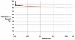
Because some UV lenses are not corrected for chromatic aberration, refocusing of the lens is necessary when using an illumination source with a spectral bandwidth of greater than 10 nm (see Fig. 1). Because of this, lens manufacturers such as Edmund Optics recommend reducing the effects of chromatic aberration with monochromatic light sources and narrow bandpass filters to improve the performance of the lens. As a result, refocusing the lens is not necessary. This approach is also used at Opto Engineering to increase the resolution and depth of field of their telecentric lens systems (see “UV lenses image fine details”).
UV telecentric lenses are not only used for industrial machine-vision measurement applications. One of the most important types of lenses used in precision laser marking systems is the telecentric UV scanning lens. Manufactured by companies such as Carl Zeiss, Sill Optics, and Special Optics, a Navitar company, these lenses exhibit a large depth of field and small spot size to ensure fine spot sizes of laser marks or drilled holes while maintaining precise placement over a relatively large field of view (FOV).
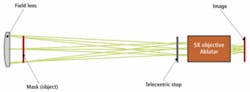
In the development of a system for the production of ink-jet plates, MicroLas Lasersystem has used such a lens—the Ablatar from Carl Zeiss—to demagnify a mask with small openings onto a polyimide foil. The images of the mask openings are used to laser ablate the foil to create drilled holes with diameters between 20 and 50 μm (see Fig. 2). These drilled foils are subsequently mounted on ink-jet cartridges. Interestingly, the performance of these ink-jet cartridges is then measured in the visible spectrum by vision systems that incorporate telecentric lenses (see “Vision system monitors ink jets,” p. 11).
Zooming in
Often, however, it is the feature sizes of the semiconductor wafers themselves that need to be imaged. To accomplish this, manufacturers such as Navitar offer UV zoom lenses such as the NanoVue 248-nm lens. Designed to work with 248-nm UV infinity-corrected microscope objectives to enable optical inspection to under 0.1 µm, the 0.75X–3X zoom lens, when fitted with a 100X objective lens, achieves a zoom range of 75–300 times. A FOV of 0.14 to 0.37 mm can be achieved using the 100X infinity-corrected UV objective with a 2/3-in. format sensor. Using the UV zoom coupled with this objective, an operator can zoom in on particular details of interest and achieve the required FOV while still resolving important image details.
Last year, Resolve Optics was selected by Channel Systems to design a UV zoom lens with a focal length of 80–200 mm for use in its Digital Cerenkov Viewing Device (DCVD) for verification of spent nuclear fuel (see Fig. 3). Because spent nuclear fuel emits a faint UV Cerenkov light when gamma rays from fuel assemblies interact with electrons in the cooling pond water, the DCVD captures the Cerenkov image of spent fuel for analysis and comparison and allows inspectors to differentiate irradiated fuel items from nonfuel items.
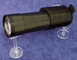
The UV zoom lens was designed and wavelength-corrected to view a nuclear fuel assembly 13 m away from the lens and through 10 m of water. Miniature motors allow remote setting of both zoom and focus functions. To enable the lens to be switched between 270- and 350-nm UV and 400–700 nm without the need to refocus the lens, a filter slide was incorporated. Using a telescopic focus, the lens can image objects from 3 m to infinity.
Matching cameras
Whether used in semiconductor fabrication and inspection or parts-inspection applications, UV lenses are playing an important role in producing and inspecting parts with high resolution. But coupling the correct CCD or CMOS camera to these lenses plays an equally important part of any system specification.
To increase the sensitivity of these cameras’ sensors in the UV, a process called backside thinning (BST) is used in which the backs of the imagers are thinned to extend the wavelength range of the imager from the visible to the UV. Already, a number of different approaches to BST have been proposed by Sarnoff, Fairchild, and the Jet Propulsion Laboratory to improve the sensitivity of both CCD and CMOS imagers in the UV region (see “CMOS cameras support fiber interfaces,” p. 11).
To optimize for sensitivity and for the lifetime of the near-UV spectrum quartz lenses, quartz windows and imagers without microlenses need to be used. For this reason, companies such as Edmund Optics and JAI already specify the types of cameras they recommend for UV-based applications.
The Edmund Optics UV megapixel 25-mm fixed-focal-length lens, for example, is suitable for imaging in the 280–365-nm wavelength range, and the company recommends its use with the XCD-SX900UV megapixel camera from Sony. The lens can also be used, without refocusing, over the entire spectral range of the visible region of Sony’s XC-EU50UV. Using monochromatic illumination and bandpass filters allows the lens to be used from 230–800 nm, with refocusing necessary for each 10-nm step in the illumination spectral output. JAI also offers cameras with or without quartz windows and/or microlenses for specific UV applications.

UV lenses image fine details
Traditionally, machine-vision lenses have operated in the visible spectrum, allowing captured images to accurately represent those seen by the human visual system. In semiconductor applications, especially, however, the limitations of the resolvable resolution that can be obtained in the visible spectrum have led to the development of lenses that operate in the ultraviolet (UV) region of the electromagnetic spectrum. Here, because the wavelength of UV light is lower than that of visible, the resolving frequency achievable by such lenses is higher, allowing finer object resolutions to be measured.
The limiting resolution of any lens is given by the cutoff or spatial frequency (expressed in line pairs/mm) at which the lens no longer yields image contrast information. As the cutoff frequency is inversely proportional to wavelength of light, inexpensive machine-vision lenses and telecentric optics operating in the visible range cannot be used with cameras that employ CCD or CMOS sensors with small pixel sizes.
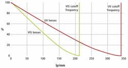
Operating in the 365–425-nm range, UV lenses provide much higher image contrast at high spatial frequencies and can be used with CCD or CMOS-based cameras that feature small pixel sizes (see Fig. 1). When used in combination with standard, lower-resolution cameras, the high resolution of these lenses means they can tolerate object displacements much larger than visible lenses before image defocusing occurs, and, thus, when compared to telecentric lenses operating in the visible spectrum, depth of field is increased.
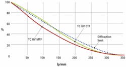
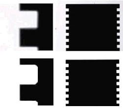
In addition to the MTF diffraction limit, both the MTF of UV lenses and the contrast transfer function (CTF) provide valuable information about achievable resolution (see Fig. 2). While the MTF curve describes the response of the lens to a sinusoidal pattern, the CTF function expresses the contrast the lens is yielding when a “square wave” pattern of black-and-white stripes is imaged. The results of comparing images taken with lenses operating in the visible and UV wavelengths are shown in Fig. 3.
While UV telecentric lenses can be used with any UV illuminators operating in the 356–420-nm range, such as ring, coaxial, and backlight illuminators, UV LED collimated illuminators provide the highest image resolution and depth of field. These telecentric illuminators ensure an efficient coupling between the UV LED source and the UV telecentric lens by backlighting the object with the most appropriate geometry. With such configurations, UV enhanced detectors are not needed, allowing any CCD- or CMOS-based camera to be used.
Claudio Sedazzari, president
Opto Engineering
Mantova, Italy
www.opto-engineering.com