IMAGE CAPTURE: GigE camera spots solar cell defects
Driven by government-funded programs such as the German “100,000 Roofs” program, solar power is one of the fastest growing alternative energy sectors in Europe. To achieve the maximum power output, the photovoltaic devices used in solar cells must be manufactured as effectively as possible to produce highly efficient products. Manual quality assurance is next to impossible as the fragile wafers are difficult to handle—even more so at the high throughput rates required for production.
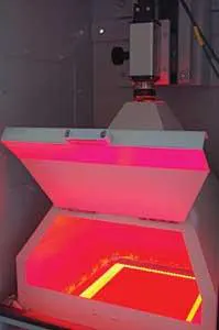
To overcome this limitation, companies such as Eckelmann (Wiesbaden, Germany; www.eckelmann.de) are developing wafer inspection systems to ensure that the polycrystalline silicon from which solar wafers are manufactured is free from chips, cracks, and broken edges that will cause power loss in finished solar panels. Currently, Eckelmann is developing a test and inspection station for a customer who wishes to equip several wafer production lines, each with a throughput of 3600 wafers/h (see figure).
To test these 0.2-mm-thick raw silicon wafers, each part must be individually tested for purity and freedom from defects. A machine-vision system inspects each wafer for flaws, chipping, and edge defects and measures its surface area and the angle of each chamfered corner at a rate of one wafer per second.
“One of the most challenging aspects of the system,” says Jan Helmerichs, a software developer with Eckelmann, “is to achieve the necessary accuracy at a throughput rate of one wafer every 0.8 s.” In the wafer inspection station, a camera is installed in a metal housing that is open at the bottom and has built-in lighting. During production, a rotary table positions the sawn silicon wafers below the camera for in-line inspection.
To capture images of the approximately 150 × 150-mm wafer at a 50-μm resolution, Helmerichs used the UI-5480-C from IDS Imaging (Obersulm, Germany; www.ids-imaging.com), a camera that uses a CMOS color sensor with 2560 × 1920 pixels and an area of interest (AOI) function for limiting the field of view to a square partial image. Image data is transmitted at 15 frames/s to the system’s host PC using the camera’s Gigabit Ethernet port. Cable lengths up to 100 m allow flexible positioning of the camera even at a large distance from the host computer.
In operation, the camera exposes two successive images, each with different lighting. First, the wafers are examined in red LED backlight to make through-cracks visible. The LED backlight consists of a frame of red LEDs covered by a diffusion plate and a glass carrier to hold the wafer. Because the LED backlight has a hole in the middle, a vacuum can be used to fix the wafer during measurement. After the backlit image is exposed, a second image is taken using diffuse incident white LED light, which clearly contrasts impurities and defects on the surface and non-through-cracks.
This image is also used for measuring the wafer size and the chamfers at the corners. While the camera takes the second image, image-analysis software based on the Halcon software package from MVTec Software (Munich, Germany; www.mvtec.com) segments the first image using grayscale operators. As image capture and analysis can be performed in parallel, this solution saves time.
The measuring system can be operated either locally or remotely through a graphical user interface called E.See Waferinspect developed by Eckelmann. According to Eckelmann, the system can be tailored for other measurements such as wafer thickness and grain size.
“Because the camera’s uEye SDK provides an interface for the Halcon software library, it was quickly integrated into the PC-based system. And, because all IDS USB and GigE cameras use the same SDK, no programming is necessary to change to a different camera model should the system need to be upgraded,” says Helmerichs.

