Uniquely Challenging

Xing-Fei He
Although the economic situation slowed down photovoltaic (PV) installation last year, the market continues to grow. According to the European Photovoltaic Industry Association (EPIA), the market will reach $31 billion with a capex of $6 billion in 2010. With oversupply of capacity, solar cell manufacturers are under pressure to find ways to increase efficiency, improve quality, and reduce costs.
Automated optical inspection (AOI) systems are growing rapidly as the solar industry is reaching the stage of maturity in which machine vision undergoes mass adoption on the production floor. A properly designed AOI can help meet these goals. At some production stages, however, AOI system designers have unique challenges to overcome.
Silicon-wafer-based solar cells currently represent 82% of the PV market, according to EPIA. The typical solar cell has a structure (see Fig. 1) that needs a variety of processing techniques to fabricate, including surface texturization and the silk-screening of conductor layers for connection of the cell into a panel assembly.
Compared with traditional semiconductor electronics manufacturing processes, wafer-based solar cell manufacture has some unique processing steps that create both opportunities and challenges for AOI. While there is no standardized production flow in the solar-cell manufacturing industry, a typical fabrication process contains opportunities for AOI to aid in error detection and process control (see Fig. 2).
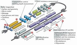
An incoming wafer inspection system looks at the surface conditions and geometry of the wafer, checking for distortion, chips, saw marks, contamination, and obvious cracks. It also looks for micro-cracks, which are especially problematic for solar cell production because they can result in a wafer shattering during the following steps. Shattering not only results in yield reduction but can shut down the production line for the time needed to remove the debris.
Other AOI opportunities include inspecting texturization, antireflective coatings, printed metallization layers, and a final operational inspection of the finished cells that takes advantage of the solar cell’s electro-optical characteristics.
Visible imaging
Conventional AOI systems using visible light can handle a number of these inspection processes. Either linescan or area-scan cameras can be used depending on the system design.
In the geometry and surface inspection stages, for instance, visible light and a monochrome linescan or TDI camera will suffice. These types of cameras allow the inspection to occur in line, as the wafer moves along the production flow. The size and type of defects for which the system is checking require cameras with resolution in the range of 2k, 4k, or 8k pixels per line with pixels 7–14 µm in size.
The linescan or TDI rate needs to be fast enough to avoid creating a bottleneck in the production flow—typically in the 20–100-kHz range depending on the throughput. In addition, antiblooming or autoexposure features are desirable to avoid image saturation.
Inspection of the antireflection coatings can also use visible light, but color camera capability is required. Under white light, the antireflective coating on the solar cell will appear blue because longer wavelengths transmit more efficiently while the shorter wavelengths still experience reflection. The exact hue and color saturation of the reflected light depends on the coating thickness.
Consequently, using the blue channel on a color linescan camera allows detection of defects as well as process-control measurement. As with the wafer inspection system, linescan cameras allow inspection of moving wafers. Color cameras with 4k- to 8k-pixel resolution and 20–40-kHz scan rates are typical.
The metallization print process is another opportunity for AOI to identify defects and provide process-control measurements using conventional cameras and techniques. Two-camera systems can be used, providing frontside and backside inspection simultaneously.
Near-infrared imaging using backlight
One of the most demanding AOI challenges is during the incoming inspection stage: checking for micro-cracks that can occur during crystal growth and wafer sawing. This is a critical checkpoint before beginning the cell processing, both to ensure yield and to reduce the occurrence of production downtime due to a wafer shattering.
However, the micro-cracks can be too small—less than 5 µm wide—to be seen during a typical surface inspection. Furthermore, cracks are difficult to detect using surface illumination because there is almost no contrast between the reflections of the crack and the surrounding silicon.
Instead, this inspection requires the use of backlighting. Because the wafer is only 150–200 µm thick and silicon is semitransparent in the near-infrared (NIR) spectrum, LED backlighting using 850–950-nm wavelengths will provide enough illumination to obtain useful images.
Under these backlighting conditions, a crack will scatter light and create a dark line against a light background that is readily detectable. Sensors need a resolution of 2–8k pixels with 7–14-µm pixel size to be able to detect these defects.
The challenge is that CCD image sensors lose quantum efficiency (QE) in NIR wavelengths, resulting in a relatively weak signal. Moreover, camera systems vary considerably in their NIR sensitivity. Some cameras exhibit as much as 30–40% QE at 900 nm while others can be much lower. Therefore, sensor and camera selection are critical in developing an AOI system for backlit micro-crack inspection.
System developers should also consider the exposure time needed to obtain a usable image under NIR backlight because this directly affects the system’s production throughput. The shorter the exposure time, the faster the production line can run at this step.
Increasing the NIR backlight intensity is one option for reducing exposure time but is limited by the availability of appropriate LED light sources. A more practical approach is to utilize a time-delay integration (TDI) sensor. These sensors utilize multiple TDI stages (as many as 100x) synchronized to the scan rate to accumulate multiple exposures at each stage. The result is the equivalent of a single line sensor with 100x of sensitivity. For example, DALSA’s Eclipse TDI has a QE of 32% at 900 nm and 96 TDI stages, which provide a combined broadband responsivity of 1950 DN/nj/cm2 at 0-dB gain.
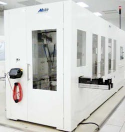
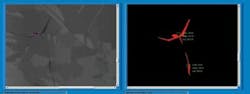
Systems for performing backlight inspections have begun to appear. For example, Meikle Automation developed the IS360 Wafer Inspector (see Fig. 3). As one of its inspection steps, the IS360 detects and analyzes micro-cracks using proprietary software and sorts wafers based on the dimension and area information of the defects (see Fig. 4). These data also provide operators with feedback to improve process control on the manufacturing floor.
Electroluminescence
Another AOI opportunity unique to solar cell manufacturing, along with backlit micro-crack wafer inspection, is final quality inspection. This step takes advantage of the solar cell’s electro-optical characteristics, which allow the cell to generate luminescence for imaging.
This step can pinpoint micro-cracks and other production-induced defects in the finished cell/panel that can cause early failure but might not be detectable via conventional electrical testing. Eliminating defective cells at final inspection can ensure that solar panels fabricated from the remaining cells have a product lifetime exceeding 20 years.
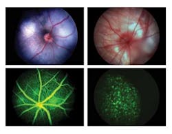
The application of a current density of about 40 mA/cm2 to a cell causes electroluminescence (EL) and results in the emission of light centered at 1.15 µm, corresponding to silicon’s bandgap energy (1.1 eV). Any defects in the silicon will appear by inspecting the uniformity of the EL (see Fig. 5). Photoluminescence (PL) uses a similar method but with laser excitation rather than an electrical current.
The EL process has the additional attribute that the amount of light a cell generates for a given applied current can serve as a measure of the solar cell’s conversion efficiency. This means the final inspection step can not only detect defects, it can help sort and grade finished cells by their output characteristics. The results can also assist in process control as well as in matching cells for compatibility in a solar panel assembly.
Handling IR insensitivity
While AOI in the final inspection has the potential to provide significant manufacturing benefits, it also represents a significant challenge for which there is as yet no ideal solution. The problem is that conventional silicon imaging sensors have extremely poor sensitivity beyond 1 µm, with a QE of almost zero.
As a result, the inspection requires long exposure times—on the order of seconds—to obtain usable images. Right now, area-scan cameras are being used in EL because of the long exposure time required and are creating a bottleneck in production.
The image sensor industry is actively seeking a better alternative. One approach is to use indium gallium arsenide (InGaAs) sensor technology, which has greater sensitivity at 1.1 µm. Unfortunately, it is also expensive. Cameras using InGaAs sensors cost from $20,000–$40,000, depending on the type of camera.
Also, the resolutions of currently available sensors—1k for linescan or 640 × 512 pixels for area-scan—are not high enough to meet the needs of these inspection applications. Imaging an entire wafer with sufficient detail would require the use of multiple cameras, multiplying the already high system cost.
An alternative is to use a fluorescent pigment coating on the silicon sensor. Infrared photons striking the coating would generate shorter-wavelength secondary photons, effectively converting the IR to visible light that the silicon sensor can more readily detect. This conversion is known as an anti-Stokes process and it has a low conversion efficiency (0.2~2%), which results in limited improvement in sensitivity requirements. The coating also could reduce the sensor’s modulation transfer function, thereby degrading sensor performance.
While the industry seeks to find a better solution to EL/PL inspection challenges, the opportunities for AOI in solar cell manufacturing remain. Many of the inspection needs can be met with fairly conventional AOI system designs and allow a tradeoff among performance and cost to match different production line needs. To address solar cell production’s unique AOI opportunities, however, developers should seek effective ways of handling NIR/IR imaging.
Xing-Fei He is senior product manager of linescan and TDI product lines at DALSA, Waterloo, ON, Canada (www.dalsa.com).
Company Info
DALSA,Waterloo, ON, Canada
www.dalsa.com
European Photovoltaic Industry Association
Brussels, Belgium
www.epia.org
ICOS, a division of KLA-Tencor
Leuven, Belgium
www.icos.be
Meikle Automation
Kitchener, ON, Canada
www.meiklesolar.com