sCMOS cameras target scientific applications

Andrew Wilson, Editor
While general purpose CCD and CMOS imagers are used in many off-the-shelf digital cameras, novel imager architectures are needed to address the needs of more specialized markets. In scientific imaging, for example, cameras must exhibit high-resolution, fast frame rates, and high-sensitivity.
Recognizing this, in 2008, a consortium of companies consisting of Andor (Belfast, Ireland;www.andor.com), Fairchild Imaging (Milpitas, CA, USA: www.fairchildimaging.com) and PCO (Kelheim, Germany; www.pco.de) embarked on a collaborative development to develop a CMOS-based architecture to meet these criteria. An imager based on the resultant technology, known as scientific CMOS (sCMOS) was introduced as a prototype one year later. Featuring a 2560 x 2160 format 6.5 x 6.5 μm pixels, the imager featured a dynamic range of 14-bits at 30 fps and a read out noise of less than two electrons at this speed (http://bit.ly/1hjdspW).
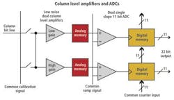
To attain this dynamic range and read out noise, the sensor features a split readout scheme of odd and even columns. As each pixel from each photo-site is read out, dual amplifiers and analog to digital converters with independent gain settings are applied to the signal and combined to achieve a high dynamic gain (Figure 1).
The design of such a sensor was first presented by Paul Vu and his colleagues at Fairchild Imaging in June 1988 (http://bit.ly/1dvMGGG). Today, the company offers image sensors based on variations of this technology that consist of the CIS1910F, a 1920 x 1080, 100fps device that features an array of 5T pixels on a 6.5µm pitch and the CIS2521F, a 2560 x 2160 device with 6.5µm pitch pixels.
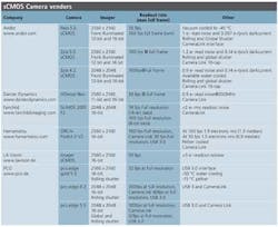
Both sensors support both rolling and global shutter modes of operation. Which mode of operation is chosen will be application dependent. In many machine vision applications, for example, where products must be imaged as they travel along a production line, motion blur can be eliminated by using a global shutter. In scientific applications, where the frame rate of the camera can compensate for any potential motion of the sample, a rolling shutter may be used. Many of the currently available sCMOS-based cameras available today support both modes of operation (Table 1).
To support the high data rates produced by these cameras, many incorporate the well-established CameraLink interface. Recently, however, the emergence of USB 3 has led some vendors to introduce cameras that incorporate this interface. While not as fast as the CameraLink interface, incorporating the USB 3 interface reduces the cost of an imaging system since no frame grabber is required as the USB 3.0 interface is now commonplace on PC-based systems. At the same, time, however, the slower USB speed leads to a lower readout rate from the camera, a limitation that may not be important in scientific applications.
In the past, such applications required Electron-Multiplication Charge Coupled Device (EMCCD)-based cameras to provide the low read out noise, high dynamic range and high-speed required. However, with the emergence of sCMOS-based cameras, such cameras will no longer dominate scientific markets.
Indeed, to highlight the performance differences between EMCCD and sCMOS cameras, Saumya Saurabh in the Department of Chemistry of Carnegie Mellon University (Pittsburgh, PA, USA;www.cmu.edu) and his colleagues compared the quantitative performance of two EMCCD cameras with three sCMOS-based cameras.
In his study, the Evolve 512 EMCCD camera from Photometrics (Tucson, AZ, USA;www.photometrics.com), the 887 EMCCD from Andor were compared with the pco.Edge sCMOS from PCO, the Neo sCMOS from Andor and the ORCA Flash 2.8 CMOS from Hamamatsu (Hamamatsu City, Japan; www.hamamatsu.com). When used to perform single molecule detection, Saurabh showed that the three sCMOS cameras evaluated are close in performance to the EMCCD cameras tested (http://1.usa.gov/1dYkrVG).
About the Author

Andy Wilson
Founding Editor
Founding editor of Vision Systems Design. Industry authority and author of thousands of technical articles on image processing, machine vision, and computer science.
B.Sc., Warwick University
Tel: 603-891-9115
Fax: 603-891-9297