Industrial Automation: Robots and vision team for photonic devices assembly
Silicon photonics is regarded as a key enabler of applications such as optical networking as the technology allows high-speed optical communications devices to be built using proven silicon manufacturing technology. Using hybrid photonic transceivers, networking systems provide high throughput at low power and offer orders of magnitude better bandwidth than electrical interconnects. These hybrid devices are composed of a number of components such as IR light sources, silicon substrates with integrated waveguides and fiber arrays that must be precisely assembled.
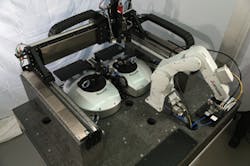
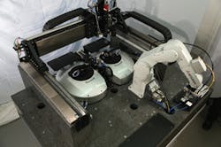
To produce pre-production batches of these devices, ST Microelectronics (Geneva, Switzerland; www.st.com) required a system that could precisely place, bond and test these individual components. By leveraging the process knowledge of The Institute of Communication, lnformation and Perception Technologies - TeCIP (Pisa, Italy; tecip.sssup.it), sub-micron positioning equipment of PI miCos (Eschbach, Germany; www.pimicos.com) and vision expertise of ImagingLab (Milan, Italy; www.imaginglab.it), PI miCos has developed a semi-automated system to achieve this task. A video of the system in operation can be seen at: http://bit.ly/1zkaT1a.
To assemble the device, a silicon substrate with optical modulators and waveguides is first combined with a bipolar CMOS circuit into a hybrid package (a process known as flip-chip bonding). After this is accomplished, the hybrid circuits are positioned in the automated system for final assembly of both the integrated laser source and the fiber array.
To accomplish this, a six-axis robot from Mitsubishi (Vernon Hills, IL, USA; http://mitsubishirobotics.com) with on-board vision, picks the hybrid circuit and places it onto an intermediate holder on a Y-stage centered between two SpaceFAB six-axis micro-positioning manipulators from PI-miCos, a mechanical device that has a resolution and accuracy of 100 nm. A 9M pixel Manta GigE camera from Allied Vision Technologies (Stadtroda, Germany; www.alliedvisiontec.com) is then used to image the hybrid circuit and the positional information of the connector block and to pass this information to the SpaceFAB manipulator.
"Since the accuracy of the machine vision system is diffraction limited," says Ignazio Piacentini, PI miCos' Director of International Programs, "only a coarse alignment can be achieved through vision." A further fine alignment, in the sub-micron range, is obtained by coupling a laser source to a power meter using two fibers positioned over a waveguide on the silicon substrate. By moving the component in a spiral search pattern using the SpaceFAB six-axis micro-positioning modules, the light power output peak is used to provide feedback to finely adjust the position of the fiber array. The fiber array is then bonded in position by means of optical epoxy resin.
The solid state IR laser module is then positioned and assembled in a similar manner. However, since the emission is in the SWIR and the beam is pointing downward, this is imaged by a SWIR GigE camera from Xenics (Leuven, Belgium; www.xenics.com) mounted in the granite base of the alignment bench.
To control the robot, motion control, machine vision and test equipment, Piacentini and his colleagues used LabVIEW from National Instruments (Austin, TX; www.ni.com). This software was also used to develop a graphical user interface (GUI) to display the status of the system to the operator. The application software also includes an editable 'sequencer' that enables the user to finely tune the whole assembly process flow.
In the current design of the system, positional height information of the hybrid circuit is acquired using a laser triangulation technique. This is used to properly position the IR and fiber arrays at the correct height on the hybrid circuit. "In future designs," says Piacentini, "micrometer scale height information may be achieved using a dedicated 3D camera.".
Vision Systems Articles Archives

