Disparate detectors enable low-light level cameras
Many different kinds of detectors are now being offered by manufacturers of low-light level cameras.
Andrew Wilson
In many scientific, security, medical and military imaging applications, it is important to capture images at very low-light levels. To do so requires image sensors that must exhibit high quantum efficiency (QE), low readout noise and dark current as well as a wide dynamic range.
In developing these image sensors, manufacturers of camera vendors are leveraging several different technologies. Generally speaking, such low-light level imagers can be segmented into two classes, either those that are photo-conductive or those that are photo-emissive. While CCD and CMOS imagers are photo-conductive, other classes of device such as hybrid devices that employ micro-channel plates (MCPs) and electron-bombarded CCDs (EBCCDs) are photo-emissive.
Conductive and emissive
In photoconductive devices, images are generated by incoming photons that are converted to electron charges at each photosite of the imager. Alternatively, in photo-emissive devices, such as the EBCCD, photons are first detected by a photocathode, and the resulting electrons focused onto a back-thinned sensor resulting in the formation of electron-hole pairs from which an electrical signal can be derived at each photosite.
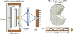
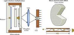
However, classing such devices in such broad terms does not fully express the number of different variations of photo-conductive and photo-emissive devices that are currently available. Many intensified CCD (ICCD) sensor systems, for example, use a combination of photo-cathodes, MCPs, phosphor screens and either CCD or CMOS imagers in their designs (Figure 1).
In such configurations, the incident photons falling on the photocathode generate photo-electrons that are accelerated towards an MCP that acts as a high-gain electron multiplier. Multiplied photo-electrons emerging from the MCP are then reconverted back to electrons by a phosphor screen and detected by a photo-conductive device such as a CCD or CMOS imager.
To transfer these images from the phosphor screen, either fiber optic or lens coupling can be used. Such ICCD/ICMOS intensified camera systems are often supplied with numerous photocathode materials to allow them to be tailored for specific spectral ranges. Similarly, different phosphor types are also available that exhibit different emitted spectrums and decay times, making the choice of photocathode material and phosphor type important when meeting the needs of any particular application.
While many camera systems employ this technology, some manufacturers supply OEM image intensification modules that can be retrofitted to general purpose CCD or CMOS-based cameras. Stanford Computer Optics (Berkeley, CA, USA; www.stanfordcomputeroptics.com), for example, has developed such a module dubbed "Quantum Leap," that can be used with a number of different optical input and output lens formats and an optional time/gain module that allows the signal gain, gating and delay time of the image intensifier module to be controlled remotely.
In such devices, the conversion of light to electrons and then back to photons is inefficient and, because of this, a number of other types of image intensification have also been developed that eliminate the MCP, phosphor screen and any fiber optic or lens coupling found in these more conventional devices.
Like a conventional image intensifier, electron bombarded CCDs (EBCCDs), for example, still require a photocathode to convert incoming photons to electrons. Once converted however, these electrons are accelerated using a high-voltage gradient onto a back-thinned CCD creating electron-hole pairs at each photosite from which the signal electrons can be collected.
Intevac (Santa Clara, CA, USA; www.intevac.com) has successfully used this technology in the development of an electron-bombarded active pixel sensor (EBAPS) that it has incorporated into the E3010M, a self-contained camera module that incorporates an SXGA 1280 x 1024 pixels (SXGA) EBAPS CMOS sensor, high and low voltage power supplies and flash memory). Designed for integration into imaging systems including head/helmet-mounted displays, rifle sights and small electro-optic optic/infrared (EO/IR) surveillance systems, the camera module is subject to ITAR restrictions.
Electron multiplication
While neither traditional ICCD systems nor EBCCD approaches could be truly termed purely solid-state approaches, the emergence of monolithic solid state imagers that use the principle of electron multiplication have emerged to overcome the limitations of number of components required. These so called electron-multiplying CCD (EMCCCDs) do not require the use of photocathodes, MCPs, phosphor screens or fiber optic coupling. Rather, gain is achieved after the incoming photon is converted at the CCD or CMOS imager by the devices themselves.
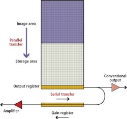
In their design, the range of Impactron devices from Texas Instruments (TI; Dallas, TX, USA; www.ti.com) and the low-light level vision (L3Vision) series from e2v (Chelmsford, England, www.e2v.com) use impact ionization to achieve this gain. Both approaches use a gain register that is integrated after the serial readout register of the sensor (Figure 2). These serial readout elements are operated at a high clock voltage and, as a result, additional electrons are generated at each transfer.
ON Semiconductor (Phoenix, AZ, USA; www.onsemi.com) has taken a somewhat different approach in the design of its KAE-02150, 1920 x 1080 CCD. Each of the sensor's four outputs incorporates both a conventional horizontal CCD register and a high gain EMCCD register. An intra-scene switchable gain feature samples each charge packet on a pixel-by-pixel basis. This enables the camera system to determine whether the charge will be routed through the normal gain output or the EMCCD output based on a user selectable threshold.
Today, a number of cameras are available that employ these EMCCD-based devices. The Falcon Blue FA285B-CL Camera Link camera from Raptor Photonics (Co. Antrim, Northern Ireland; www.raptorphotonics.com), for example, employs a Peltier-cooled 1Mpixel frame transfer Impactron imager from TI to provide a quantum efficiency of up to 65% for low light applications such as fluorescence, X-ray and hyperspectral imaging. For its part, Andor Technology (Belfast, Northern Ireland; www.andor.com) incorporates a 1024 x 1024 EMCD from e2v in its latest iXon Ultra 888 back-illuminated EMCCD-based camera that offers single photon sensitivity at speeds of up to 26fps.
To further increase the sensitivity of these EMCCD devices, Photometrics (Tucson, AZ, USA; www.photometrics.com) and Princeton Instruments (Trenton, NJ, USA; www.princetoninstruments.com) have worked with e2v to develop a series of CCD/EMCCD sensors that use a patented back-thinned process called eXcelon to reduce etaloning - a phenomenon that is caused by light passing through the CCD, being reflected at the rear surface and producing interference fringes when reflected light interacts with incoming waves.
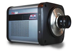
When the technology is applied to EMCCD devices, the result is detectors with minimal etaloning. These devices are featured in Princeton Instruments' ProEM+ series of deep-cooled EMCCD cameras with 512 x 512, 1024 x 1024 pixel formats and 1600 x 200 and 1600 x 400 formats for spectroscopy applications (Figure 3). Because EMCCDs use a gain register that effectively multiplies the charge from weak signals before readout noise is added by the output amplifier, the effect of read noise is reduced.
Dynamic range of all image sensors is a measure of the full well capacity of the device divided by the smallest signal that can be measured. In an EMCCD, the smallest signal is the read noise of the device divided by the multiplication gain. Thus, increasing the gain of the device will result in an increased dynamic range.
CMOS sensors
Although the benefits of single photon-sensitive devices such as EMCCDs will continue to dominate extremely light starved applications, the emergence of sCMOS-based cameras over the past few years is challenging EMCCDs for less demanding applications. Introduced in 2009 by Andor Technology, Fairchild Imaging (Milpitas, CA, USA; www.fairchildimaging.com) and PCO (Kelheim, Germany; www.pco.com), the design of sCMOS imagers do not use the principles of electron multiplication to increase dynamic range. Rather, as the signal from each photosite is read out, a high gain, high sensitivity amplifier is applied to obtain the lowest possible noise on one output and a low gain amplifier applied on another output to obtain the largest possible signal. These signals then read simultaneously and converted into digital values and combined into a high dynamic range signal.
To highlight the performance differences between EMCCD and sCMOS cameras, Saumya Saurabh in the Department of Chemistry of Carnegie Mellon University (Pittsburgh, PA, USA; www.cmu.edu) and his colleagues compared the quantitative performance of two EMCCD cameras with three sCMOS-based cameras. In his study, the Evolve 512 EMCCD camera from Photometrics the 887 EMCCD from Andor were compared with the pco. Edge sCMOS from PCO, the Neo sCMOS from Andor and the ORCA Flash 2.8 CMOS from Hamamatsu (Hamamatsu City, Japan; www.hamamatsu.com).
When used to perform single molecule detection, Saurabh showed that the three sCMOS cameras evaluated are close in performance to the EMCCD cameras tested (http://1.usa.gov/1dYkrVG). (see "sCMOS cameras target scientific applications," Vision Systems Design, March 2014, http://bit.ly/1f6h9CW).
Bigger pixels
Since dynamic range is directly proportional to the full well capacity of the device, using larger pixels with lower spatial resolution can also be used to increase dynamic range. Recognizing this, Anitoa Systems (Palo Alto, CA; www.anitoa.com) has developed a CMOS imager that features an array of 24 x 24 active CMOS pixels each 150μm x 150μm in size. Excessive noise that cannot be eliminated in the chip due to is filtered using a proprietary software algorithm, that the company calls "Intelligent Dark-current Management."
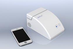
Partnering with Zhejiang University of China (Hangzhou, Zhejiang Province, China; www.zju.edu.cn), Anitoa has recently demonstrated the use of the device in a handheld medical device to detect molecular interactions based on fluorescent or chemical luminescence imaging (Figure 4).
Of course, several other methods also exist to extend the dynamic range of image sensors. These can be classified into those that modulate the exposure time of the pixels and those that modulate the conversion gain of the pixels. Today, numerous companies offer such devices and cameras that employ them (see "CMOS imagers look to increase dynamic range," Vision Systems Design, October 2014; http://bit.ly/1r1tett).
When choosing a low-light level camera for any particular application, systems developers must weigh numerous factors including speed, dynamic range, field of view and spatial resolution. The numerous detector types and camera offerings now available may at first present a challenge to those wishing to purchase a low-light level camera. Luckily, there are numerous online references that accurately describe the differences between detector types and cameras and the performance that can be expected from them (see "Low-light-level imaging on the Web", on this page).
Low-light level imaging on the Web
Impactron-A New Solid State Image Intensifier
http://bit.ly/1MlM4r4
Electron-Bombarded Charge-Coupled Devices (EBCCDs)
http://fla.st/1Q79aY8
Electron Multiplying Charge-Coupled Devices (EMCCDs)
http://fla.st/1IdpGyu
What Is EMCCD Technology
http://bit.ly/1GyzxOq
CCD, EMCCD and ICCD Comparisons
http://bit.ly/1ePPJ5n
High Sensitivity Cameras: Principle and Technology
http://bit.ly/1Q79mqd
Electron Multiplying CCD Technology: The new ICCD
http://bit.ly/1MlNZf3
EMCCD Technology in High Precision Photometry on Short Timescales
http://bit.ly/1JqJVua
New-generation CCD/EMCCD technology-A review of eXcelon technology
http://bit.ly/1MlOfL3
Scientific sCMOS image sensors
http://bit.ly/1hjdspW
Electron bombarded back-illuminated CCD sensors for low light level imaging applications
http://bit.ly/1deThgi
EMCCD vs. sCMOS for Microscopic Imaging
http://bit.ly/1KN11Ew
Unravelling Sensitivity, Signal to Noise and Dynamic Range - EMCCD vs. CCD
http://bit.ly/1KN2drz
Electron Multiplying CCDs- New Technology for Low Light Level Imaging
http://bit.ly/1AKBKHV
