Electronics manufacturing: Multi-sensor system inspects printed electronics
By printing electrically-conductive inks onto foil, paper or glass substrates, electronics, manufacturers can create active or passive devices that are thin, flexible and low-cost. To create these devices, conventional printing methods such as screen and inkjet printing can be used.
"After such devices are printed," says Yair Kipman, President of ImageXpert (Nashua, NH, USA; www.imagexpert.com), "they must be inspected to ensure that they will perform in the correct manner." This entails checking whether the deposited tracks are of the correct width, whether they are broken or have rough edges, or whether any excess ink material (known as satellites) may have been deposited between the tracks.
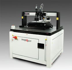
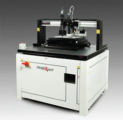
To analyze these features, ImageXpert has developed a fully-automated imaging system that integrates multiple cameras and sensors to perform measurements. To begin analysis, the flexible sheet of printed electronics is placed onto a 24 x 24in X-Y positioning stage from Aerotech (Pittsburgh, PA, USA; www.aerotech.com) that is mounted with a vacuum chuck to ensure that the circuit will remain perfectly flat during image scanning.
To image the components printed on the material, the X-Y table is indexed in 2in swaths and the reflected images captured from above by two separate cameras. The first, a Mako GigE area array camera from Allied Vision (Stadtroda, Germany; www.alliedvision.com) fitted with a 19in 6:1 telecentric lens from Moritex (San Jose, CA, USA; www.moritex.com), is used to image patterns such as fiducials that serve as a point of reference for image measurements.
"Depending on the material to be imaged," says Kipman, "this lens system can be used with either coaxial illumination or diffuse on-axis illumination systems to allow both specular and non-specular materials to be imaged correctly."
To capture a high-resolution image of the printed circuit, the sample is then illuminated by a white on-axis line-light from Metaphase Technologies (Bristol, PA, USA; www.metaphase-tech.com) and images captured by a 4k x 1 Racer line-scan camera from Basler (Ahrensburg, Germany; www.baslerweb.com) fitted with a telecentric lens from Opto Engineering (Mantova, Italy, www.opto-engineering.com). As the X-Y table moves, line-scan images are transferred over the cameras GigE interface to the host computer.
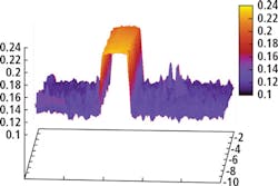
"As well," says Kipman, "it is often important to measure the volume of ink that has been deposited along each track since this will determine the amount of current that can flow through the printed circuit." In such applications, an LK-G32 CCD laser displacement sensor can be mounted on the system to create two-dimensional profiles of each track as the X-Y table moves. Multiple 2D profiles can then be combined to generate a 3D image of the track and thus the volume of conductive material deposited can be calculated.
ImageXpert has developed a set of image processing tools to calculate parameters such as line width, raggedness, volume and whether any satellites or broken lines may be present. Expanding on the Visionscape software from Microscan (Renton, WA, USA; www.microscan.com), ImageXpert's user interface allows an operator to view and measure these parameters.
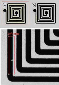
In a demonstration at the company's headquarters, Kipman showed how these tools could be used to measure features of a printed antenna. First, the number of connected dark pixels in the image is determined, their total area computed and the result compared with a known good value. Should the value be less than the known good value, then the electrical tracks that compose the antenna may be broken.
Similarly, by placing a region of interest (ROI) around the tracks, the raggedness of a line can be measured by computing the line deviation. By setting specific tolerances, the system can then flag the user if the part is not acceptable.
"In some applications, such high-resolution 1 micron/pixel images are not required," says Kipman. For these applications, ImageXpert also offers a system based around an 1100XL flatbed scanner from Epson (Suwa, Nagano, Japan; www.epson.com). Capable of achieving a 10 micron/pixel resolution, the system can be used to detect features such as track width, broken tracks and line widths on printed electronic circuits.


