Camera design: Image sensor technology enables very low light imaging
What do detecting a fluorescent marker viewed under a microscope, an image of the retina captured with an ophthalmic fundus camera, or a surveillance image operating on a cloudless, moonless night have in common? All require image sensor technologies that enable very low light imaging, 30 fps image capture, and illuminations down to 0.1 lux.
Historically, Electron Multiplication Charge Couple Device (EMCCD) technology has been successful in enabling the capture of scenes with very low light levels. This technology takes the very small charge detected in a pixel under low light and multiplies it many times before reaching the sensor's amplifier. While this technology excells - even down to the detection of single photons - the electron multiplication cascade can overflow and create blooming artifacts if signal levels entering the EMCCD register are too high, limiting use of sensors with this technology to scenes that do not contain any bright components.
Interline Transfer EMCCD technology addresses these limitations directly by combining the low light sensitivity available from an electron multiplication output register with the image uniformity, resolution scaling, and electronic global shutter capabilities of Interline Transfer CCD. This combination enables the development of image sensors that can capture continuously from very low light to bright light in designs that can range to multiple megapixels in resolution.
"Key to the performance of this technology is an Intra-Scene Switchable Gain feature, which avoids overflow in the EMCCD output register under bright illumination conditions by selectively multiplying only those portions of the scene that require it," explains Michael DeLuca, Go to Market Manager, Industrial and Security Division, Image Sensor Group, ON Semiconductor (Phoenix, AZ, USA; www.onsemi.com).
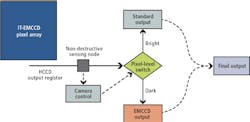
The output design shown (Figure 1) illustrates how the charge from each pixel passes through a non-destructive sensing node that can be read by the camera control electronics to provide an initial measurement of the signal level for each pixel. This information is used to drive a switch in the sensor that routes charge packets to one of two outputs based on a camera-selected threshold.
Pixels with high charge levels (corresponding to bright parts of the image) are routed to a standard CCD output for conversion to voltage, while pixels with low charge levels (corresponding to dark parts of the image) are routed to the EMCCD output for additional amplification before conversion to voltage.
These two datasets are then merged to generate the final image. Because the charge from pixels with high charge levels does not enter the EMCCD register, this output architecture allows both very low light levels and bright light levels to be detected while avoiding the image artifacts associated with overflow of the EMCCD output register.
The power of this technology can be seen in Figure 2, which shows image captures of a single scene that includes both a bright light as well as very dark shadows, where the darkest portion of the image is illuminated only by moonlight or starlight.
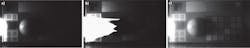
A traditional image sensor (Figure 2a) images the bright part of the image well, but doesn't have the sensitivity to "see" in the very darkest part of the image. A traditional EMCCD (Figure 2b) can be configured to image in the very darkest part of the scene, but when the gain is turned up to enable this low light imaging, artifacts from the bright part of the scene destroy the image integrity. Interline Transfer EMCCD technology (Figure 2c) allows the scene to be imaged continuously from the brightest to the darkest part of the image, where "dark" can extend all the way down to illumination only by moonlight or by starlight.
Having been moved forward from the research labs to use in production devices, Interline Transfer EMCCD technology is being used today in a growing family of products. For example, ON Semiconductor's KAE 02150 image sensor uses Interline Transfer EMCCD technology to enable low light image capture at 1080p (1920 x 1080) resolution while operating at 30 fps, making this device well suited to security, surveillance, and situational awareness applications that require high sensitivity image capture with video frame rates.
For higher resolution needs, the 8 MPixel (2856 x 2856) KAE 08151 image sensor is designed in a square aspect ratio with a 22 mm diagonal, aligning with the native optical format of many scientific microscopes and other medical equipment. "By leveraging the advances available with Interline Transfer EMCCD technology," DeLuca concludes, "these devices are the first in a new class of image sensors that achieve high levels of performance under low lighting conditions."