Scientific-grade imagers boost CCD sensitivity
Superior noise and resolution parameters enable CCD sensors to handle demanding scientific applications.
By Andrew Wilson,Editor
Many CCD cameras used in machine-vision applications use broadcast-resolution CCD imagers to capture images at 25 or 30 frames/s. Although such cameras are reasonably sensitive, their quantum efficiency, readout noise, and dark count make them unsuitable for applications such as fluorescence, chemiluminescence, and confocal microscopy.
To provide superior spatial resolution and higher image fidelity than interline video cameras in these applications, developers of high-performance CCD cameras are turning to scientific-grade CCD sensors. In addition to featuring variable exposures, these cameras use large, high-resolution CCDs, offer 12-, 14-, or 16-bit dynamic range, feature region-of-interest capture and pixel binning, and often are cooled below room temperature to lower readout noise and dark count.
Lowering noiseSignal-to-noise ratio (S/N) is one of the most important parameters to be considered when specifying a CCD camera for scientific applications. Three sources contribute to this ratio: photon, dark, and readout noise. Although many of these noise sources can be reduced by camera design and cooling methods, photon noise or photon shot noise—the inherent natural variation of incident photon flux—cannot be reduced by camera design.Unlike photon noise, dark noise within a CCD is produced by electrons thermally generated within the structure of the CCD. Because the largest contribution to this dark current results from the interface between the silicon dioxide (SiO2) and the epitaxial silicon (Si) layer within the CCD, full-frame CCDs can be operated in multiphase pinned mode (MPP) to reduce this effect. The Si/SiO2 interface at the surface of the CCD is pinned at the substrate potential, directing signal charge away from the Si/SiO2 interface toward the buried n-channel. This reduces dark noise, increases charge-transfer efficiency, and increases pixel-to-pixel uniformity.
Designed for fluorescence, Raman, absorbance, and emission applications, PixelVision (Tigard, OR) CCD detectors for spectroscopy feature front- and back-illuminated CCDs, with imaging formats of 532 x 64 to 1100 x 330 pixels and a 16-bit dynamic range at 50 to 100 kHz. At the heart of many of these systems is a thinned, back-illuminated CCD that uses multiphase pinned clocking to reduce dark current.
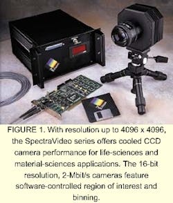
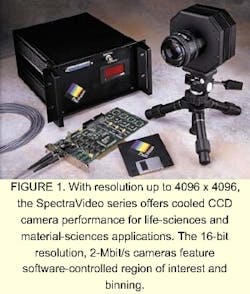
Also available is a 14-bit high-speed platform with data rates to 40-Mpixels/s (80 Mbytes) sustained bandwidth, allowing capture of up to 3000 frames/s. A variety of front- and back-illuminated CCDs are available ranging from 80 x 80 to 2048 x 2048 formats. (see Fig. 1).
Hole-accumulation-diode (HAD) photosites used in interline-transfer CCDs have the same effect as MPP clocking. Several devices that use HAD technology have been incorporated into CCD cameras. These include the CoolSNAP color camera from Roper Scientific (Trenton, NJ). Using the 1392 x 1040 ICX205AK color interline progressive-scan HAD CCD with microlenses from Sony (Park Ridge, NJ), the camera incorporates thermoelectric cooling to achieve a dark count of 14 electrons/s at 20°C.
Lowering temperatureDue to impurities in a CCD's silicon layer, some pixels suffer from dark current more than others. These so-called "hot pixels" build up thermal electrons at a much faster rate than the majority of pixels in the CCD. To reduce dark current caused by these pixels and others across the device, the CCD can be cooled. To accomplish this, the sensors used in scientific-quality cameras are cooled either by forced-air, thermoelectric (using Peltier coolers), or cryogenic means. For every 6°C reduction of temperature, dark current reduces by a factor of two.CCD cameras that have Peltier, or thermoelectric, coolers are common among scientific CCD cameras. These cooling devices are, in essence, solid-state heat pumps that, with the application of electrical current, transfer heat from one side of the device to the other. While the amount of heat reduction they can achieve varies, the temperature differential between the two sides lowers the dark current of the CCD sensor dramatically.
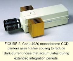
In the design of the 4920 monochrome CCD camera from Cohu (San Diego, CA), for example, Peltier cooling reduces dark-current noise that accumulates during extended integration periods (see Fig. 2). The sensor operates at 5°C in a 25°C ambient environment, resulting in a reduction of dark current to about one-eighth of that without cooling. Using a Peltier cooler, along with a natural-convection, dual-section heat sink, the sensor collects more light to display as a reduced-noise video image.
Of course, in applications such as astronomy, where ultralow readout noise and ultralow dark-current noise are required, cryocooled-liquid and liquid-nitrogen sensors must be used. Companies such as PixelVision offer products such as the SpectraVideo camera that provide read noise as low as four electrons rms and dark current as low as 1 electron/s. In the SpectraVideo series, a number of cooling configurations are available, including multiple-stage thermoelectric and liquid cooling. With software control of binning, region of interest, analog gain and bandwidth, clock rates, and row transfer timing, the cameras are supplied with a PCI-based frame grabber and Windows-compatible acquisition software.
Quantum efficiencyCCD sensors are not equally sensitive to all wavelengths of light. The spectral sensitivity of CCD sensors, or quantum efficiency (QE), is different for each CCD at every wavelength. Quantum efficiency is the percentage of photons converted to electronic signal. The higher the QE, the more sensitive the device.In general, the photosensitive area of a frame-transfer CCD is completely covered with polysilicon gates for charge transportation. Front-illuminated devices have no response in the UV spectrum, because the polysilicon gates absorb the input light. Absorption losses also occur in the visible spectrum causing a reduction in sensitivity. To enhance the ultraviolet response, a phosphorus coating (lumogen) can be applied.
Alternatively, thinned, back-illuminated CCDs can be used to increase the QE. In a back-illuminated CCD, the CCD is turned over and processed to remove the substrate so that light enters the pixels from the rear of the pixel structure rather then through the gated electrodes on the front side. This arrangement raises the QE to more than 80% for the wavelengths from 550 to 800 nm.
In the design of its AP7 CCD camera system, Apogee Instruments (Tucson, AZ) uses a 512 x 512 back-illuminated CCD to achieve an 85% peak QE, with a 65% QE at 400 nm (see Fig. 3). The camera, targeted at scientific and astronomy applications, can digitize 16-bit pixels and features a greater-than-85-dB dynamic range. To attain these parameters, the camera is cooled using a liquid-nitrogen cryostat or a unique mechanical cryogenic cooler. In operation, CCD temperature set point is adjusted, and CCD temperature is determined under computer control.
Increased sensitivityAnother method to increase the S/N in scientific camera systems is pixel binning. In this method, adjacent pixels are added together to form a superpixel. As well as increasing the sensitivity of the imager, S/N will increase since the effects of individual photons or electrons (known as shot noise) will be reduced. With this increased sensitivity, users benefit from a reduced integration time, but, since fewer total pixels result, the trade-off between increased sensitivity for lower resolution must be balanced.According to Apogee, binning is a good method for focusing, because image acquisition speeds up greatly while giving greater sensitivity to lower out-of-focus light levels. A KAF-0400 CCD sensor from Kodak (Rochester, NY) having 796 x 512, 9-µm-square pixels, for example, can appear to have 398 x 256, 18-µm-square pixels with a binning of 2 x 2. With 3 x 3 binning, the sensor appears to have 265 x 170 pixels with a size of 27 µm square and nine times the sensitivity. At 3 x 3 binning, a KAF-1600 will appear as 512 x 341 pixels, each 27 µm square.
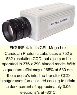
Canadian Photonic Labs (Minnedosa, Canada) uses this technique in its CPL-Mega Lux C90 CCD cooled camera (see Fig. 4). Featuring 16-bit data conversion, the camera's 752 x 582-resolution CCD also can be operated in 376 x 290 binned mode. With a quantum efficiency of 65% at 530 nm, the camera uses an interline-transfer CCD imager that has fan-assisted cooling to attain a dark current of approximately 0.05 electrons/s at -30°C.
In addition to considering factors such as device types, readout speeds, S/Ns, and quantum efficiency, systems integrators must weigh other technical factors before considering the purchase of a CCD camera for scientific applications. These include exposure times, dynamic range, resolution, software support, and cost. While much of this information can be found on the Internet, perhaps the best evidence of a camera's effectiveness is whether it has been successfully deployed by others in specific applications such as confocal imaging, astronomy, or ophthalmology.
Company InformationDue to space limitations, this Product Focus does not include all of the manufacturers of the described product category. For information on other suppliers of scientific CCD cameras, see the 2001 Vision Systems Design Buyers Guide (Vision Systems Design, Feb. 2001, p. 82). Apogee InstrumentsTucson, AZ 85715Web: apogee-ccd.comCanadian Photonic Labs
Minnedosa, Manitoba
R0J 1E0, Canada
Web: www.cplab.com
Cohu
San Diego, CA 92123
Web: cohu.com
Kodak Image Sensors
Rochester, NY 14650-2010
Web: www.kodak.com
PixelVision
Tigard, OR 97223-4310
Web: www.pv-inc.com
Roper Scientific
Trenton, NJ 08619
Web: www.roperscientific.com
Sony
Park Ridge, NJ 07656
Web: www.sony.com


