IC vendors tailor imagers to meet demands
As the battle of CMOS versus CCD imagers subsides, sensor vendors are tailoring their devices to specific applications.
By Andrew Wilson, Editor
Since their introduction more than 30 years ago, charge-coupled devices (CCDs) have all but eliminated tube-based image sensing in applications in machine vision, remote sensing, broadcast television, and security. Originally conceived as a computer-memory replacement, the low-cost, high-resolution, ruggedness, and stable image quality that can be obtained from today's CCDs have created new applications in biosciences, astronomy, medical imaging, and forensic research.
Despite the long history of CCDs, the architecture of these devices has remained relatively consistent over the last decade. CCDs are now available in many configurations that include linear, time-delay integration (TDI), and area arrays.
LINEAR DEVICES
Linear devices are often used for applications such as desktop scanners and photocopiers, where the imager is generally moved across the object to be scanned in a "push-broom" manner to capture a two-dimensional (2-D) image. In web-inspection applications, these imagers are incorporated in linescan cameras, where a fixed stationary camera analyzes or captures the motion of a fast-moving 2-D area of metal, plastic, or woven material.
TDI-based designs build on this linear architecture by using a number of linear rows of photodiode detectors. This allows multiple exposures of the moving object to be accumulated while effectively increasing the integration time available to collect incident light. Systems developers can use TDI-based camera designs to increase the speed of the web while reducing the need for dc-based halogen lighting.
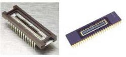
Many companies, including Dalsa, Kodak, and NEC Electronics America, currently offer linear CCDs. Their product lines include monochrome devices, color imagers, and TDI devices for web inspection (see Fig. 1).
To digitize color images, companies offer linear CCDs as an array of three parallel element photodiodes, designed to digitize primary RGB components. Targeted at color linescan applications such as color scanners, Kodak's KLI-2113 sensor consists of three parallel 2098-element photodiode arrays—one for each primary color. Independent exposure control for each channel allows color balancing to be performed at the front end of the device, reducing later processing requirements.
Like color imagers, TDI devices use a number of parallel arrays. Rather than detect color, however, these linear elements are designed to combine multiple exposures of the same scene, increasing sensitivity and reducing the amount of lighting needed in web-inspection applications. For example, Dalsa's IT-F6 is a 2048 × 96-line TDI sensor that features eight 20-MHz taps and 13 × 13-µm pixels with a 100% fill factor.
AREA ARRAYS
Full frame, frame transfer, and interline transfer are the most popular architectures now found by designers specifying area array devices for imaging applications. Each of these architectures is different and meets specific imaging applications.
Full-frame imagers consist of a parallel CCD shift register, a serial CCD shift register, and an output amplifier. Using this architecture, high-resolution, high-density CCD imagers can be fabricated because none of the silicon area is occupied by light-shielded areas or transfer arrays. However, because the parallel register is used for both image detection and readout, a mechanical shutter or synchronized strobe illumination must be used to properly capture images.
The AP series of cameras from Apogee Instruments support a range of CCD sensors up to 4096 × 4096 pixels from both Atmel and Kodak. These full-frame CCD sensors are used in conjunction with shutters from Vincent Associates and Melles Griot to achieve exposure times as fast as 0.020 s.
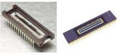
The e2v technologies CCD47-10 is another example of a full-frame imager. Designed for scientific, spectroscopic, and medical-imaging applications, the device features a 1024 × 1024-image format, an image area of 13.3 × 13.3 mm, 13-µm square pixels, and a 100% active area (see Fig. 2). With a single serial output register, the device incorporates separate charge-detection circuits at each end of the register, which is split so that a line of charge can be transferred to either output or split between the two.
To achieve continuous operation without the use of strobe or shutters, CCD vendors also offer a number of frame-transfer devices. Similar in design to full-frame devices, these imagers add an identical parallel storage register that stores the readout from the photosensitive area of the device. Because this parallel storage array is as large as the active imager area, the resolution of such devices is generally less than their full-frame device counterparts and their cost higher.
One of the latest developments from Texas Instruments is its TC285SPD Impactron, a frame-transfer CCD image sensor that features multimode readout capability. Progressive scan, interlaced scan, and line summing are all supported on the 1004 × 1002-pixel imager that can be shuttered from 1/30 to 1/5,000 s. With a peak quantum efficiency of 60%, the device is already in use in the company's EVM285SPD camera, created both as an evaluation unit for the TC285SPD sensor and for machine-vision and image-processing applications. The cooled-CCD evaluation module outputs thirty 1-Mpixel frames/s and features adjustable charge multiplication gain control, electric shutter, 2 × 2 column/row binning, and image averaging.
INTERLINE TRANSFER
Rather than add a large single-storage array to imagers, many manufacturers offer interline CCD devices that separate the lines of photosensitive regions of the CCD with light-shielded parallel readout CCDs. While this overcomes the problems of adding shuttering or strobes (as in the case of full-frame devices) and eliminates the need for a storage area, it results in lower sensitivity because a smaller photosensitive area is present at each pixel site.
For the broadcast market, such interline-transfer imagers are offered with an interlaced output. In this mode, even and odd fields are successively read from the device so that the output remains broadcast-compatible. Although useful in surveillance applications where cameras must remain compatible with broadcast standards such as NTSC and PAL, these imagers are often avoided by machine-vision camera designers.
Because charges from even and odd lines of the imager are transferred at different times, imaging high-speed objects with these CCDs can result in image frames with shifted odd and even fields. This lag between even and odd fields can be overcome by progressive-scan, noninterlaced interline designs, in which the entire imager is reset before integration, charges are transferred to light-shielded areas, and shifted out of the sensor. Such imagers are better suited for machine-vision camera designs, in which odd and even rows of the imager cannot be allowed to have different integration times.
Interline-transfer devices designed for solid-state camera applications are available from several vendors including Sony Semiconductor. The company's IXC 422AL, for example, is a 2/3-in. interline CCD imager that features a field period readout system, 768 × 494 effective pixels, and an electronic shutter with variable charge-storage time.
IMAGER SPECS
In specifying CCD sensors for a specific image-processing application, camera vendors must not only weigh the types of devices that are available but also their performance characteristics. These include fill factor, signal-to-noise ratio (S/N), quantum efficiency, readout noise, dynamic range, and dark count.
In consumer applications such as toys and mobile telephones, these parameters may not be very important. But in scientific and industrial applications such as semiconductor inspection, color machine vision, and astronomy, understanding these parameters is an important part of specifying any imaging system.
Quantum efficiency, for example, is a measure of how well a specific sensor responds to different wavelengths of light—the higher the quantum efficiency (%), the more sensitive a CCD will be at any given wavelength. Standard front-illuminated CCDs are generally more sensitive to green, red, and IR wavelengths than they are to blue. In astronomy applications, color wheel-based imaging will therefore require longer exposures with a blue filter to achieve a properly balanced image.
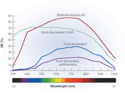
To increase the quantum efficiency in such applications, CCD camera vendors often use back-illuminated devices. CCDs such as the SI003AB and SI502AB from Scientific Imaging Technologies (SITe) use this technique to achieve 85% quantum efficiency, over 20% higher than their front-illuminated CCD equivalents (see Fig. 3).
CMOS CHALLENGES
Despite the advances that have been made in CCD fabrication, the structure of these devices has changed little. Over the past few years, the emergence of a new type of image sensor fabricated in complementary metal-oxide semiconductor (CMOS) technology promised higher performance, lower power, higher levels of integration, and lower cost.
For years, the arguments over the advantages of image sensors that use CCD technology versus those manufactured with CMOS fabrication processes have raged. Fueled by marketing hype, many people were led to believe that CMOS imagers would replace CCD sensors in nearly every imaging application. Manufacturers' data sheets claimed that their CMOS imager was comparable, if not equal in performance, to CCD devices.
Unfortunately, none of this was true. And rather than replacing CCDs, CMOS imagers found new markets of their own—consumer cameras, mobile telephone/cameras, toys, and other devices that do not demand the image quality well known to designers of CCD cameras. Several technical factors hindered the acceptance of CMOS devices in high-performance machine-vision applications. These included high fixed-pattern noise, low S/N, low fill-factor, and (despite the marketing hype), the fact that CMOS imagers could not be easily fabricated using "standard CMOS" wafer fabs.
RANDOM ADDRESSING
To be fair, however, the CMOS imager has found applications apart from consumer products. In high-speed imaging, for example, the random pixel addressability of CMOS devices has meant that regions of interest on imager chips can be clocked at rates exceeding the capability of CCD devices. Random addressing can exchange frame speed for image resolution, allowing windowed frame rates of thousands to millions of frames per second.
This has led to the introduction of a number of high-speed CMOS-based imaging cameras targeted at applications such as automobile crash testing. And, because CMOS sensors can be built with logarithmic photoelectric transfer, a dynamic range beyond six decades (120 dB) can be obtained by log-compression of the input optical power scale onto a linear output voltage scale. In this way, devices can observe scenes with vastly different luminance in the same image, without the need to set an exposure time. Again, this is proving useful, especially in surveillance and automotive applications where embedded cameras may be required to operate over a large dynamic range.
To address the needs of these applications, companies such as Fillfactory, Photonfocus, and SmaL Camera Technologies offer CMOS devices with a high dynamic range. Photonfocus, a company whose Linlog technology was developed at the Swiss Federal Institute of Technology, for example, has now commercialized the technology, introducing a number of CMOS imagers and cameras (see p. 35).
Created with a process similar to memory circuits and processors, the main advantage of CMOS imagers is the additional functionality that can be integrated onto a single device. Already, in high-volume consumer applications the sensors have been integrated with on-chip timing, automatic gain correction, output registers, and analog-to-digital converters. These devices are already finding use in low-cost machine-vision sensors where simple machine vision functions need to be performed (see p. 15).
NOVEL ARCHITECTURES
The high degree of systems-level integration and random accessibility of CMOS imagers is also allowing researchers to explore novel imaging architectures that may better model the human visual system. At the University of Waterloo, Faycal Saffih and Richard Hornsey have developed a pyramidal CMOS image sensor that models the parallel 2-D image acquisition of the fovea.
At the University of Genova, Giulio Sandini and his colleagues have developed a retina-like visual sensor that features a space variant resolution similar to the human retina. The CMOS device uses a log-polar structure in which a constant number of photo sites are arranged in concentric rings. According to Sandini, the structures allow high-resolution images to be captured at the central region while allowing the lower-resolution information at the periphery to provide relevant background information.
Rather than displace the CCD as the imager of choice in multiple applications, CMOS devices have already carved their own market niches adding functionality and lowering cost in low-light-level, high-speed, and low-cost machine vision sensors. In many scientific, military, medical, and machine-vision applications, however, the performance characteristics of CCD devices remain superior.
Company Info
Apogee Instruments, Auburn, CA, USA www.ccd.com
Atmel, San Jose, CA, USA www.atmel.com
Dalsa, Waterloo, ON, Canada www.dalsa.com
e2v technologies, Chelmsford, UK www.e2vtechnologies.com
Fillfactory, Mechelen, Belgium www.fillfactory.com
Kodak, Rochester, NY, USA www.kodak.com
Melles Griot, Rochester, NY, USA www.mellesgriot.com
NEC Electronics America, Santa Clara, CA, USA www.necel.com
Photonfocus, Lachen, Switzerland www.photonfocus.com
Scientific Imaging Technologies (SITe), Tigard, OR, USA www.site-inc.com
Sony Semiconductor, San Jose, CA, USA products.sel.sony.com/semi/
SmaL Camera Technologies, Cambridge, MA, USA www.smalcamera.com
Swiss Federal Institute of Technology, Zurich, Switzerland www.iqe.ethz.ch
Texas Instruments, Dallas, TX, USA www.ti.com
University of Genova, Genova, Italy www.unige.it
University of Waterloo, Waterloo, ON, Canada www.uwaterloo.ca
Vincent Associates, Rochester, NY, USA www.uniblitz.com