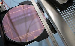
Big chip suits medical imaging applications
A UK consortium has developed a CMOS imager for medical applications that is claimed to be 200 times larger than the devices found in today's PCs and laptops.
The 12.8-cm-square DynAMITe (Dynamic range Adjustable for Medical Imaging Technology) imager -- which was built using 0.18-micron CMOS technology -- is claimed to be the largest device that can be made on a single industry-standard 8-in. (20-cm) diameter wafer.
Led by Nigel Allinson, Distinguished Professor of image engineering at Lincoln University (Lincoln, UK), the MI-3 Plus consortium that developed the device was funded by the UK Engineering and Physical Sciences Research Council.
It comprised a group of engineers from University College London and the University of Surrey as well as physicists at The Institute of Cancer Research (ICR) and The Royal Marsden Hospital, who are now investigating potential applications for the device.
-- Posted by Vision Systems Design
