Andrew Wilson, Editor, [email protected]
The rapid decrease in feature sizes on semiconductor wafers, data-storage devices, and other microelectronic components has created a need to extend the resolution limit for optical inspection. The current trend is to drop further down into the shorter wavelengths. “To achieve 0.1-mm resolution,” says William Bridson, director of new product development at Navitar (Rochester, NY, USA; www.navitar.com), “parts must be imaged at the 248-nm deep-ultraviolet (DUV) wavelength.”
Reflected DUV is viewed using specialized lenses made of materials such as fluorite and quartz that will transmit the 248-nm wavelength. Specialized cameras, sensitive to this wavelength, are also required. In the design of its BX2-DUV upright optical microscope, for example, Olympus America (Melville, NY, USA; www.olympusamerica.com) has developed a system that uses sophisticated lighting, lens systems, and positioning stages to image parts in the 0.25-0.1-μm range.
To image wafer features, parts are placed on a stage and viewed through a series of objectives. The features are located with normal objectives in visible light, then the illumination is switched to the UV, and the DUV objectives are placed in the optical path. To facilitate remote changing of the objectives, the lenses are mounted on a rotary turret that can be controlled automatically from the system user interface.

“These lenses are not inexpensive,” says Bridson, “because it is difficult to produce a well-corrected optical system using only two types of material.” Leica (Wetzlar, Germany; www.leica-microsystems.com) has a 100X objective, for example, that is priced at about $27,000.” Other DUV objectives will reach up into the high $40,000 range. Adding to this cost is the expense of providing a narrow-bandwidth 248-nm wavelength. In lieu of a laser, a 100-W mercury xenon lamp is used, along with suitable blocking filters, to produce the required wavelength characteristics.
After filtering out most of the light from the arc lamp, a low-light sensor is required to capture images. This implies a large pixel for optimum light collection. A general rule is that at least two pixels must be used for the system to resolve a specific feature. When resolving features of 0.1 μm using image sensors with 0.1- and 14-μm pixel pitches, it takes considerable magnification to overlay two pixels. Not only is it impractical to produce a high-magnification objective, but the small field of view becomes cumbersome to use.
To provide magnification of up to 5X greater than that of the objective, Olympus, for example, provides three different relay magnification lenses for its system. Offered in 2.5X, 3.5X, and 5X magnifications, the lenses increase system magnification and ensure that adequate detail is resolved.
“To attain different magnifications, the operator must manually swap these lenses to alter the achievable resolution of the system,” says Bridson. Rather than take this approach for OEMs in the semiconductor industry, Navitar announced a-0.75X-3X zoom lens (NanoVue 248) at Semicon West ( July 2005; San Francisco, CA, USA).
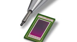
“By replacing fixed-focus lenses with a single zoom relay lens, the operator no longer has to change magnifier lens systems to compensate for detail characteristics. The added flexibility of a zoom system permits maximizing the field of view while still resolving the detail. At about $10,000, the lens can be coupled with cameras using 2/3-in. format sensors and C-mount adapters. Navitar has demonstrated its system based on this technology using a collection of optical components from Leica, Mitutoyo America (Aurora, IL, USA; www.mitutoyo.com), Olympus, and its own 0.75X-3X relay zoom lens (see photo).
Unfortunately, these systems are about an order of magnitude more expensive than visible-light inspection systems. The benefit is being able to resolve detail that was only viewable with electron microscopes. As semiconductor linewidths shrink, use of shorter wavelength will likely increase, resulting in an increase in the cost of OEM components used to evaluate them.