Named after Professor Joseph Petzval, a 19th century Hungarian mathematician and physicist, Petzval field curvature describes an optical aberration where the sharpest focus of the lens is on a curved surface in the image space rather than a plane. While careful optical design can reduce this field curvature, combining the different types of optical elements required to do so may result in a more expensive lens.

While such aberrations can be compensated for optically, developing a sensor with a curved, spherical surface can accomplish the same task while allowing simpler lens systems with lower numbers of optical elements to be used. As result, there will be an increase in light intensity at the sensor and a reduction in vignetting effects at the peripheral of the lens. In developing such systems, camera vendors may substantially reduce the cost of their products by eliminating the cost of expensive lenses used in conventional systems.
Such concepts, however, are not new. Six years ago, for example, Professor Yonggang Huang at Northwestern University (Evanston, IL, USA; www.mech.northwestern.edu) collaborated with Professor John Rogers, at the University of Illinois at Urbana-Champaign (Urbana, IL, USA; http://illinois.edu), to create an array of silicon detectors and electronics that could be conformed to a curved surface. To do so, Rogers created a hemispherical transfer element made out of a thin elastomeric membrane. Planar photo-detectors were then transferred onto the elastomer and the elastomer shaped to a hemispheric form.
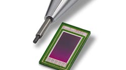
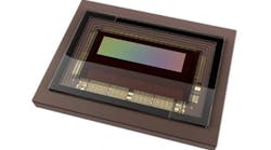
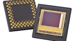
Rather than take this approach, a number of commercially available products are now emerging that use curved solid-state imagers to reduce field curvature. At the Vision 2012 trade show in Stuttgart, for example, Andanta (Olching, Germany; www.andanta.de) showed how such image sensors could be designed in the form of a one-dimensional cylindrical curvature or as a two-dimensional spherical curvature. As part of a customized project, the company has already realized a front illuminated 4k x 4k image sensor with convex and concave surfaces. According to the company, its curved image sensors are currently not yet available as standard devices, but could be developed on custom request.
Needless to say, the benefits of this concept have also been widely recognized by other companies. At this year's Symposia on VLSI Technology and Circuits Conference, held in Honolulu from June 9-13, for example, researchers at Sony (Atsugi-shi, Japan; www.sony.com) described an imaging system comprising a hemi-spherically curved, back illuminated CMOS image sensor with an integrated lens. According to Kazuichiro Itonaga, a device manager with Sony's R&D Platform, the imager/lens system doubles the sensitivity at the edge of the image circle and by a factor of 1.4 at the center of the image circle.
Although few details were announced about the manufacturing process used to create the device, Itonaga said that the device achieves the same level of curvature found in the human eye according to a recent report in IEEE Spectrum. In that article, Rachel Courtland reported that two such devices had been announced, one measuring 43mm in diameter for digital cameras and another, an 11mm diagonal device for mobile telephone applications (see "Sony Creates Curved CMOS Sensors That Mimic the Eye," http://bit.ly/1lmf02a).
Vision Systems Articles Archives