by Nicholas Sischka, Director of Imaging Product Development at Edmund Optics, and Kyle Firestone, Technical Marketing Engineer at Edmund Optics.
The advancement of machine vision technology is continually driven by ever-more increasing demands for higher performance. Integrators consistently require vision system components with better resolution and with less space, weight, and price sacrifices. The most cutting-edge applications will always require the highest performance specifications, influencing manufacturers to push the limits of what is physically possible to measure, let alone manufacture. With this consideration in mind, optical engineers, designers, and manufacturers must pay close attention to the marginal increase in technological demands, year over year, to ensure continued service to customers with relevant and useful products.
Over the course of just five years, the number of available machine vision camera options with sensor formats larger than 1 in but smaller than 35 mm has drastically increased for integrators. Today, resolutions for machine vision cameras containing the ever-more commonly adopted APS-C, APS-H, and 35 mm machine sensors formats, typically range from 32 to 250 MPixels. These resolutions continue to trend to larger numbers by way of increasing format sizes, among some other factors. The increased adoption of these larger sensor formats is a direct result of the increase in performance quality attributed to changes in the manufacturing processes. These changes have occurred in sensor illumination technology, pixel sizes, and the size of available sensor formats, amidst and despite the backdrop of a global supply chain shortage of semiconductors for many camera manufacturers.
Sensor Relative Illumination
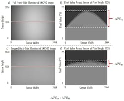
The manufacturing process for pixels on camera sensors balances performance with fabrication convenience. For this reason, before 2022, the majority of sensors featured front-side illumination (FSI) technology rather than back-side illumination (BSI); the latter of which features superior illumination uniformity but would come at a much greater difficulty to fabricate (Figure 1).
Pixels on sensors consist of three main constituent layers. The order in which these layers are stacked differs between the FSI and BSI type sensors (Figure 2).
On both sensor types, the first layer consists of a number of microlenses. Each microlens functions to gather a greater number of light rays than would be possible without the lens by increasing the acceptance angle for each pixel. These microlenses bend the rays and direct the light to the specific area on the sensor associated with each corresponding pixel. The cumulative effect of the increased etendue, or light throughput per pixel, improves the overall sensor signal and, as a result, the contrast of the sensor across the full field. For color sensors, a color filter array (CFA) is the layer just below the lenses but is not present for monochrome cameras. Sensor microlens arrays are not a new technology though and were common for machine vision sensors before 2022.
However, BSI for machine vision sensors was not common before 2022. This illumination type differs from the more common FSI type by changing the order of the second and third layers. The second FSI layer and third BSI contain the various metal and semiconductor electronics associated with the photovoltaic conversion of photon signals to electronic signals. The third FSI layer and second BSI layer are the photo-diode substrates and contain the photo-receiving surfaces at the top-most component of the layer (Figure 2).
BSI structured sensors feature a highly superior relative illumination (RI) uniformity due to less light ray obstruction. In BSI sensors, light only passes from the first layer onto the light-sensitive region of the photodiode in the second layer. Conversely, for light to be incident on the sensitive region of the photodiode of an FSI sensor requires the rays to pass through an attenuating layer of semiconductors and electronics. For FSI sensors, this attenuation is seen as a reduction in RI at the corners of the sensor (depicted in Figure 1a and consequently less so in Figure 1c).
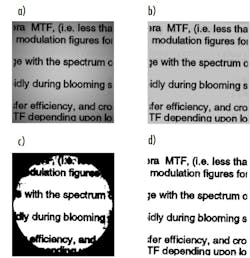
As previously mentioned, FSI sensors are the more prevalent sensor type on the market and used in machine vision imaging because of the ease with which they are manufactured. However, because of advancements in microlithography manufacturing methods, BSI sensors are becoming more commercially available. This performance increase because of the increase in RI uniformity enables superior sensor contrast levels across the full area of the sensor (Figure 3).
While contrast and resolution are not the same measurement, they are inextricably linked. Resolution without either an explicit or implicit contrast is meaningless, and the modulation transfer function (MTF) is what links these two specifications.
Contrast, Resolution, and the MTF
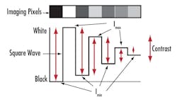
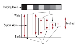
Contrast is the difference in intensity of the grayscale values between two neighboring pixels, typically reported as a percentage. The overall contrast of an image is determined by setting the brightest and darkest gray values of the image as the maximum (IMAX) and minimum intensities (IMIN). This is shown in Equation 1 and (Figure 4).Perfect black and white values are impossible to attain unless there are errors in the system. Machine vision lens manufacturers must set a contrast convention to compare the resolution of one lens to another. This convention is typically set at a minimum of 20% but may slightly differ between manufacturers.
Resolution
Resolution is a term that is used colloquially to mean a variety of different concepts and can be measured for each individual component, any number of ordered components, and the entire set of components constituting an imaging system (Table 1).
For machine vision, resolution is generally defined as the frequency (or number) of resolvable line pairs over a designated linear dimension, typically represented in units of line pairs per millimeter (lp/mm) and specified for either image or object space. The Nyquist frequency, which is the absolute upper limit of the resolution for a camera sensor, is calculated by assuming there to be one line pair per pixel pair. The equation for this resolution is given in Equation 2.
Pixel Size
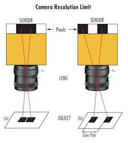
There are primarily two different ways that sensor manufacturers increase the number of pixels on sensors and therefore increase resolution. The first method for this is by decreasing pixel size. However, this comes with a number of optical and electronic limitations. Smaller pixels are typically much more sensitive to environmental factors such as ambient temperature or electromagnetic fields, which increase Johnson noise. The second main complication to this guideline is the diffraction limit or physical limitation on the optical components in the system. This limit is the resolution limit to which an imaging lens can physically render an image of two discernably distinct objects (lines, on pixels, for example) without the two objects blurring together as indistinguishable. The diffraction limit given in Equation 3 is a function of the wavelength of light used to illuminate the object, λ, and F-number of the lens, f/#. (Figure 5).
Note: ∅Airy Disk is the diameter of the Airy Disk image appearing on the sensor. The constant 2.44 comes from the first zero of the first order of the Bessel function of the first kind, J1(x), divided by π. The size of the Airy Disk can be thought of as the minimum sized pixel that a diffraction limited optical system could view as its maximum frequency.
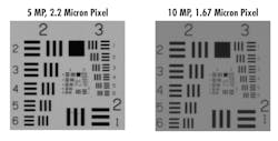
Thus, to understand the performance of an imaging system, it is important to first understand what each specification is quantifying. Though camera manufacturers tend to emphasize the importance of having as many megapixels as possible, signal-to-noise ratio of the sensor and performance of the imaging lens used are by no means whatsoever inconsequential and are at least as important as the pixel count if not more (Figure 6).
Image quality is an umbrella term that can mean several different things. It is defined by the needed requirements of the application. While the pixel count of a sensor is important to know, qualities such as image contrast have much more to do with the physical performance limitations of the optical and electronic components in lens and camera system.
Growing Sensor Sizes
The second, more common, way that sensor manufacturers increase the number of pixels on sensors and therefore resolutions is by increasing the overall size of the sensor. Increasing sensor sizes present challenges that differ greatly from the challenges of smaller pixel sizes. However, most challenges associated with manufacturing larger sensors are overcome by the communication, cooperation, and collaboration between the sensor and lens manufacturers.
With increases in sensors sizes comes an increase in size, weight, and power (SWaP) for imaging lenses. While machine vision cameras tend to have nearly uniform bulk densities and form-factors aspect ratios close to unity, this is not the case for imaging lenses.
Lens Size
Constructed of a series of glass elements as well as metal fixtures and assemblies, imaging lenses require users to exercise additional consideration to the specific demands and constraints of their applications such as the amount of usable, free space.
The comparison of the last two lenses of Table 2 shown in Figure 6 clearly demonstrates that an increase in resolution to similar fields of view (FOV) on two different sensors requires considerable changes to the design and, therefore, SWaP of the lens.
Camera and Lens Mounts
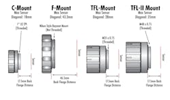
Machine vision camera sensors larger than 4/3 in. require larger alternatives to the C-Mount to ensure the full sensor is illuminated. They also need more robust, stabilized alternatives than bayonet style mounts like the F-Mount. For these reasons, machine vision camera and imaging lens manufactures have adopted the TFL Mount and TFL-II Mount (Figure 7).
The strengths of the TFL-Mount and TFL-II Mounts (referred to as TFL style mounts), are their similarities to the widely used C-Mount standard. These mounts have the same 17.526-mm flange distance as the C-Mount as well as a threaded camera interface for stability.
Considerations and the Future
The newest sensors on the market outperform most legacy models. Newer sensors provide higher resolutions, more dynamic range, shorter latency, larger sized formats, and smaller pixels than the previous generations. Because of the demands for increased imaging capabilities, imaging lenses must be carefully selected to ensure compatibility and performance optimization. Note that selecting a sensor with a larger image format, rather than one with smaller pixels, will almost always yield a larger increase in performance than vice versa. Pay close attention to the demands of the application to ensure the best machine vision camera and imaging lens pair.
