ELECTRONICS INSPECTION: DUV cameras target semiconductor inspection applications
TheCCD and CMOS image sensors used in many of today's industrial machine-vision cameras operate in the 400-to-900-nm visible light spectrum. Specialized imagers that operate in the infrared (IR) spectrum have been introduced for applications such as glass inspection, fruit classification, and plastics recycling.
For example, in semiconductor photolithography applications wheredeep-ultraviolet (DUV) light from high-power lasers with wavelengths from 190 to 370 nm produces 2-nm feature sizes, more precise measurements that can be obtained using UV-based cameras with high quantum efficiency (QE) are desirable. For such applications, very few manufacturers offer CMOS or CCD imagers or cameras that can meet these requirements.
"One of the reasons for this," says Paul Stanton, president ofAlacron, "is that the QE of unmodified commercially available frontside-illuminated sensors falls to nearly zero at wavelengths below approximately 400 nm." This low sensitivity renders them useless for DUV semiconductor inspection applications. Worse, the DUV equipment used to illuminate wafers and semiconductor masks requires high-power lasers. This damages the silicon crystal structure of the image sensor and decreases the device's sensitivity over time.
To increase the QE of image sensors, a number of different techniques can be applied. The first is to employ backside-illuminated sensors in which incident photons are collected on the backside of the sensor. Since the readout electronics are then behind the photodetectors, the fill factor of the photosite is increased to nearly 100%, resulting in a higher signal-to-noise ratio and an improved QE.
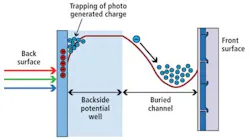
Even with such advantages, tests at a national laboratory have revealed that an effect known as quantum efficiency hysteresis (QEH) rendered the sensors unstable (see figure). Incident photons impinging on the surface of the detector result in the generation of electron-hole pairs, in which the holes (in red) become trapped at the surface of the device. Thus, as successive images are captured, they will be of variable sensitivity.
To overcome this buildup, scientists have proposed a number of techniques including UV flooding, the addition of a platinum flash gate, the addition of a metal catalyst, and delta doping. The most successful technique -- delta doping (patented) -- adds a layer of boron-doped silicon very near the back surface of the imager.
As photons disassociate into electron-hole pairs in the main body of the silicon, the holes move to the boron-doped Si layer and are transferred from the surface of the imager while the electrons are read out from the front surface. This increases the sensitivity, stability, and quantum efficiency (QE) of the device, resulting in sequentially captured images having the same sensitivity.
Recognizing the advantages of this approach, Alacron has embarked with a national laboratory upon the development of a number of DUV-based cameras based on backside-illuminated CMOS imagers. To accomplish this, Alacron first purchases 8-in. wafers of 2056 x 1560, Dynamax Dyn0032 3.2-Mpixel frontside-illuminated CMOS imagers fromPanavision Imaging.
After adding a handle wafer, these wafers are processed into backside-illuminated, back-thinned CMOS imagers, each with a delta-doped layer and an antireflection coating.
This proprietary coating can be deposited into different thicknesses over the delta-doped layers to provide a QE greater than 50% at the desired DUV wavelengths. Using chip-on-board technology, these devices are then mounted onto a 23 x 23-mm PCB and mounted into Alacron's FC-300 UV camera.
According to Joseph Sgro, PhD and CEO of Alacron, initial tests of this camera have shown a sensitivity 7-15 times greater than with a frontside-illuminated device at DUV wavelengths. The sensor can withstand thousands of pulses of 100× saturation energy level from a high-power laser over days with no measurable degradation in the sensor, the delta layer, or the antireflection coating. The FC-300 BSI version capable of 200 frames/sec will be shipped with a Full Camera Link interface later this year.
Realizing that semiconductor vendors require even higher speed, the company has also begun developing its second generation of DUV cameras that will employ a larger-format imager capable of 1000 frames/sec speed with readout speed of 8 Gpixels/sec. To read out data from the camera at these rates, the camera will employ industry-standard SNAP12 twelve-channel fiber interface transmitter modules.

