HIGH-SPEED IMAGING: Clever CMOS imager makes high-speed cameras smarter
Recent advances in CMOS imagers have led to their deployment in a number of low-light-level and high-speed cameras. By integrating circuitry to perform functions such as correlated double sampling to reduce noise, logarithmic circuits to increase dynamic range, and color-processing functions, designers are allowing camera developers to offer relatively low-cost cameras with on-chip image-processing functions.
Indeed, one of the main advantages of using CMOS technology to produce imagers is the ability to integrate image-processing functions on-chip. In many CMOS imager designs used in high-speed cameras, analog signals are digitized off-chip by analog-to-digital converters within the camera. After conversion, these digital signals are often transferred to a frame grabber where low-level functions such as convolution operators are applied, for example, to perform functions such as edge detection.
“This low-level image processing involves operations using local masks that are spatially dependent on other pixels around the processed pixel,” says Dominique Ginhac of the Cognitive Sciences Research Unit at the University of Bruxelles (Bruxelles, Belgium; http://srsc.ulb.ac.be). “The digital image processing is computationally intensive and requires a high bandwidth between the image memory and the digital processor.”
By using an analog or a mixed-approach, however, smart image sensors can be developed that offer superior performance and are smaller, faster, and exhibit a lower power consumption than a combined image sensor and image processor. These can then be used to develop high-speed cameras with on-chip image-processing capabilities.
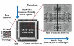
To accomplish this, Ginhac and his colleagues have developed a 64 × 64-pixel imager/processor device that can capture images at up to 10,000 frames/s and run low-level image-processing functions between 2000–5000 frames/s. What is unique about the device that Ginhac has developed is the way that local operators are performed using analog circuitry (see Fig. 1).
In the design of the device, each of the processing cells on the device consists of four photodiodes that are used to capture light. As these analog signals are captured, two analog memories, together with amplifier and multiplexer structures, are used as intelligent pixel memories that can dissociate the acquisition of the frame held in the first memory and the processing of the previous frame (held in the second memory).
To perform image-processing operations on these analog signals, four analog multipliers act as an arithmetic logic unit (ALU) that performs the linear combination of the four adjacent pixels using a 2 × 2 convolution kernel. Because each multiplier takes two analog signals and produces an output, image-processing operations such as spatial convolution can be performed by using one of the inputs as the value of the kernel coefficient and the other to corresponding pixel value.
Of course, the larger the size of the convolution kernel used the smaller the edge frequencies detected in the image. Often, convolution kernels such as the Sobel operator are used for this purpose. One particular implementation uses a pair of 3 × 3 kernels to detect gradient changes in both the vertical and horizontal axes of the image. To accomplish this in Ginhac’s CMOS imager/processor, the convolution kernel is first decomposed into two 2 × 2 masks that successively operate on the image.
“Dynamically assigning coefficient values allows the device to be reconfigured for a number of image-processing algorithms,” says Ginhac. “The on-board ALUs also decrease the number of single operations such as additions and multiplications that need to be executed by an external FPGA.”
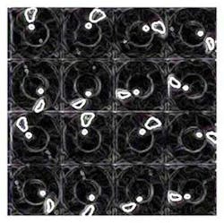
To test the device, Ginhac and his colleagues developed a camera using the device and imaged a sequence of 16 images of a fan rotating at 3750 rpm (see Fig. 2). As can be seen, by applying the on-chip Sobel filter, the camera could clearly distinguish the two white markers placed on the fan.
null


