Dual cameras evaluate ceramic circuit boards
Inspection workstation integrates imaging hardware and software to compare digital data with stored templates for assessing multilayer boards.
By R. Winn Hardin, Contributing Editor
Kyocera America Inc., LTCC Division (Beaverton, OR), manufactures printed-circuit boards (PCBs) for, among others, a customer that supplies commercial aircraft with in-seat wireless communication systems. These high-frequency systems require more than standard plastic circuit boards, however. "Ceramic circuit boards have higher conductivity and lower loss and dielectric constant than other types of boards, which makes the material ideal for high-frequency components in communication systems," explains Kyocera LTCC Division general manager David Hester.
Similar to common plastic-type boards, low-temperature cofired ceramic (LTCC) circuit boards are made up of several thin layers with metal traces that form the circuits. Layers connect to other layers through metal-filled, mechanically punched holes called vias. The layers are then laminated into a single board and fired in an oven. After firing, the ceramic material is harder than plastic.
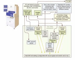
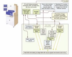
FIGURE 1. The Midas CC-1000 vision-inspection workstation archives defect images and map locations of ceramic printed-circuit cards in an ASCII database stored on the PC host. Color still images from a Sony XC55 CCD camera can be added to the archive with the inclusion of an optional frame grabber card in the PC and a cable-connection from the Sony monitor output to the frame grabber. Image-processing functions are conducted by the three proprietary boards in the image-processing assembly, a box that resides between the PC host's parallel port and the Dalsa linescan camera. Most of the template matching is done by Altera field programmable gate arrays for high-speed processing.
During processing, however, the ceramic material can become deformed and not entirely planar, making its high-resolution 2-D inspection a challenging task. However, the primary problem for automated optical inspection systems in this application is that metal traces are difficult to discriminate from the ceramic layers because of their lighter color and different material properties. Consequently, Kyocera turned to systems-integrator Midas Vision Systems (Foxboro, MA, USA) for a vision-inspection system that incorporates a Dalsa (Waterloo, ON, Canada) linear array camera, a custom processing engine, four halogen light sources, and a Sony Electronics (Park Ridge, NJ, USA) CCD color camera to provide real-time review of PCB defects (see Fig. 1).
Adaptable templates
Kyocera's Hester chose the Midas CC-1000 off-line 100% inspection workstation to help refine the ceramic printing process. "What we'd like to do is use the CC-1000 to improve the process so that we reach a point where we only have to audit the boards rather than remain at 100% inspection," Hester says. After several months of trial use, the vision-inspection system is meeting its requirements.
The CC-1000 workstation is a host PC-based system that uses a standard desktop PC with a Pentium processor and a monitor and runs on Windows 2000 Professional with a minimum of 256 Mbytes of RAM, a CD ROM drive, a zip drive, an Ethernet connection, and an Opto22 (Temecula, CA, USA) board with eight optoisolated I/O ports. The host mainly acts as the operator interface and database storage unit for the review of defects after inspection. All of the image processing is conducted by a separate image processor assembly (IPA) that connects to the Dalsa CT-E4-4096 linescan camera.
The IPA contains three proprietary boards: a template board that stores the "golden part" template in a bit-map format; a camera board that stores the digital image data from the Dalsa camera and makes pixel-to-pixel comparisons of the stored template against the acquired images using Altera Corp. (San Jose, CA) FPGA (field-programmable gate array) processing; and a RISC processor board. The IPA connects to the 4096-pixel linescan camera via an RS-422 cable and to the host PC via the 25-pin parallel port.
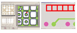
According to Kyocera's general supervisor Kevin Horton, a key advantage of the CC-1000 is its ability to create a 'golden image' from CAD data. The system offers a CAD2Midas software option that converts CAD-based data on Gerber274X files into templates. After that, Horton says, the CC-1000 YieldMax software on the PC allows the operator to map the template design into a number of regions and program-specific tolerances for individual areas or traces (see Fig. 2).
FIGURE 2. During card inspection, Midas YieldMax software displays defects in two modes: a digital representation that compares the scanned image to a template and "stop-and-stare" images of the defect (live video). The operator uses either or both displays to make card pass/fail decisions during operator review mode (left). Midas ATG2 advanced template generator software produces templates that can differentiate between 'imperfect but usable' and 'unusable' circuit patterns. Three different design features are colorized to show different defect types (right).
The 'golden image' technique implies an inspection strategy based on how close a part is to 'perfection.' The ATG (advanced template generator) software can process to the next level by producing templates that can differentiate between 'imperfect but usable' and 'unusable' circuit patterns. This flexibility allows a single technology to be effective in both process development and full-scale production applications," explains Midas LTCC market manager Ben Arnold.
Polarized defects
Because some cards become deformed during the punch-hole process to produce the vias, they are all inspected for this possible fault. After the template has been established, the operator manually loads a ceramic layer, or green card with metal traces, into the CC-1000's mini-enclosure. When the enclosure door is closed, an inspection process is triggered by a vacuum system that is connected by an optoisolated low-voltage-differential-signaling (LVDS) cable that runs from the CC-1000 to the Opto22 card in the host PC.
A vacuum fixture embedded in a Neat (Salem, NH, USA) SAS recirculating table's linear x/y stage on the base of the enclosure grabs the printed-circuit card and pulls it flat for inspection. Midas manufactures the enclosure and vacuum system using standard machine vacuum fittings and components from SMC Corp. of America (Indianapolis, IN, USA), which ties the CC-1000 workstation into the Kyocera plant vacuum generator.
The operator triggers system operation and energizes the four white halogen lights that reside at each of the four corners of the enclosure's top surface. Light from each lamp is polarized by a linear, laminated, polarizing filter. Polarized light then illuminates the card's surface area. Light reflecting off the card's metal traces retains its polarization while light reflecting off the ceramic surface becomes diffuse. The reflected light passes up and through a Schneider Optics (Hauppauge, NY, USA) photographic 90-mm lens assembly and a Midas-developed beamsplitter. The beamsplitter sends 90% of the incident light through a second polarizing filter to the Dalsa linescan camera. The remaining light is diverted to the Sony XC55 color 'stop-and-stare' camera and is not filtered. Using an optoisolated LVDS cable, the PC controls the linear stage table, which, in turn, moves the card in a serpentine manner until the linescan camera has completely imaged the card's surface area.
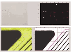
The Sony color camera, which is connected to a Sony monitor via coaxial cable, allows the operator to review any region of interest on the card at a lower resolution (640 × 480 pixels) without a loss of brightness or of contrast enhancement that comes from filtering out the crosspolarized light. The Dalsa 4096 × 1-pixel linescan camera combined with the 90-mm lens delivers resolutions down to 0.25 mil. When a defect is found by the CC-1000, digitized high-resolution images from the linescan camera are stored at the operator's request along with the card's map coordinates, and defect-analysis data are placed in an ASCII database that resides in the PC. "Stop-and-stare" images also can be stored locally by adding an optional frame grabber in the PC and feeding the video data from the Sony camera to the PC, Arnold adds (see Fig. 3).
Improving processes
According to Kyocera's process engineer Tuyen Duong, cards are produced in batches that are associated with one particular layer in the overall circuit board. The batch is then inspected by the CC-1000 one card at time, with each inspection taking about 25 s. Those cards with defects are later taken to a rework area. Reviewing the rework requirements—including the stored images of each defect and of each card with map information showing defect types and locations—speeds up the reworking process. Also, because the information is remotely accessible through the plant's local-area network, Duong can review defect data on a daily basis from his office PC and tweak the card printer to improve the overall process yield.
According to Arnold, the CC-1000 registers the stored BMP template to the card under inspection using fiducials, vias, or edges. The template is then adjusted, and the Altera FPGAs make high-speed pixel-to-pixel intensity comparisons. When the traces exceed the dimensional parameters set in the YieldMax software, the card area is flagged as a defect. The CC-1000 sorts defects into several categories including: empty or overfilled vias, pattern shorts, spacing violations, contamination/debris, opens, neck-downs, pinholes, pattern misregistrations, and excessive screen stretches.
"The results we've seen have been good," said Kyocera's Duong. He and his associates would like to see improvements made to the enclosure system, to make card loading easier, and faster processors to reduce scan times. In response to customer requests such as these from Kyocera, Midas is building a new inspection system that incorporates a more rigid granite stage to allow finer-resolution scanning and higher operating speeds. "To scan images at a 2.5-µm resolution, we need a granite-based inspection platform with the latest technology. The market has accepted the advances we have made in this area." ..
features, advantanges, benefits
David Hester, general manager at Kyocera America Inc., LTCC Division (Beaverton, OR, USA), says, "We produce complicated, close-tolerance, low-temperature cofired ceramic (LTCC) substrates. LTCC is only one possible solution to the packaging requirements of our customers and must be cost-competitive with other potential solutions. These substrates are made by laminating and cofiring multiple green cards into an array stack. The high number of circuits and features on each card makes manual inspection virtually impossible. Defects on the individual circuit layers can produce visual or electrical rejects and cause the loss of an entire array of parts. These defects must be detected in the individual circuit layers so that the rejection of a layer occurs at its lowest-cost state, instead of rejecting a completely cofired, high-cost array of parts.
"The Midas Vision system has lowered our manufacturing costs by detecting potential rejects at the initial steps of our process. It inspects for a multitude of print defects such as circuit shorts, spacing violations, contamination, circuit opens, pinholes, and pattern-registration errors. In some cases, the system has doubled our production yields. It supports our needs during system start up and operator training and has met all of our specifications," he adds.
Company Info
Altera Corp. www.altera.com
Dalsa www.dalsa.com
Kyocera America LTCC Division www.kyocera.com
Midas Vision Systems Inc. www.midasvision.com
Neat, Division of Danaher Motion Precision Systems Group www.danaherprecision.com
Opto 22 www.opto22.com
Schneider Optics www.schneideroptics.com
SMC Corp. of America www.smcusa.com
Sony Electronics www.sony.com/videocameras
CORRECTION
For the Profile in Vision Solutions article in May, p. 29, company information is:
Algus Packaging Inc. www.algus.com
Dukane Corp. www.dukane.com/us
Keyence Corp. of America www.keyence.com
Omron Electronics LLC www.omron.com/oei


