Dual-camera system zeros in on PCB defects
Printed-circuit boards (PCBs) are made by applying thin wires of metal, often in multiple layers, to a substrate. With advancing technologies, the wires that are laid out are only tens of microns in width, so exacting production is extremely critical. One method of production is to first lay out the circuit design onto a piece of specialized plastic using lasers to etch lines in the desired pattern. The plastic is then adhered to the substrate in a process to form the etched lines on the PCB.
Because breaks and bridges between metal wires that measure 10 to 100 µm can short a PCB, systems-developer MicroCraft (Raleigh, NC, USA; www.microcraftcorp.com) was asked to design an automated inspection system to find and categorize these defects. Existing methods required an operator to evaluate an image projected onto a wall with an overhead projector and to circle defects on the sheet. The operator determined the type of defect, estimated the defect size, and logged the information. No more than 10 samples could be completed in an eight-hour work shift.
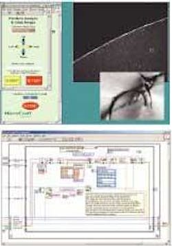
In the development of an automated inspection system to find and categorize defects in plastic film used in PCB production, MicroCraft created a front panel for motion-system control, ROI selection, and defect inspection and naming (top). Developed using National Instrument IMAQ image-processing library and LabVIEW software, the IMAQ virtual instrument block diagram shows defect detection, calibrated measurement, and image file saving, including sample code used to detect, measure, evaluate, and save the defect image (bottom).
Howard Foster, MicroCraft project engineer, developed a two-camera inspection system using large- and small-field-of-view (FOV) cameras and crosspolarized light filters to highlight defects in acquired images. Foster used a Kodak (Rochester, NY, USA; www.kodak.com) ES 1.0/MV BW megapixel camera with Navitar (Rochester, NY, USA; www.navitar.com) 7000 adjustable zoom lens set at 0.3x for the large-FOV camera and a 6.4x lens combination from Mitutoyo (Aurora, IL, USA; www.mitutoyo.com) on a SC-ST30 monochrome camera from Sony (Park Ridge, NJ, USA; www.sony.com/videocameras) for small-FOV inspection. The large-FOV camera initially inspects the film to find defects using the crosspolarized fields. The single-FOV camera is used for a secondary evaluation of the defects by the operator and to capture images and measurements for data storage.
A backlight table with enough area to support an 8-in.-diameter sample covered with a polarizing sheet is placed on a two-axis linear rail system to provide motion of the sample. The linear rail stage is controlled by a National Instruments (Austin, TX, USA; www.ni.com) PXI industrial PC with PXI-7324 motion card and two 1407 and 1422 PXI IMAQ frame-grabber cards.
After the operator places and orients a sample for correct polarization, the system automatically scans the sixteen 2-in.-square quadrants of a PCB sample with the large FOV camera. Then, using National Instruments IMAQ image-processing library and LabVIEW software, the inspection system determines the center of the suspected defect and commands the table to move so that each defect is in the FOV of the small FOV camera. To make correct location assignments to the suspected defects, Foster used several IMAQ inspection routines to counter lens problems such as pin cushioning and barreling.
After the suspect is located using the small-FOV camera, a live image is presented to the operator. The defect can then manually reject the suspect or can classify the defect and make calibrated measurements for area, length, and width. The resolution achieved with the small-FOV camera was calculated using IMAQ Vision Builder and a USAF Resolution target to be 1.17 µm/pixel. With this resolution, the system detected and quantified defects in the 10–100-µm range.
If the suspect is a defect worth cataloging, the operator names and classifies the defect and stores its image, and the image is saved to a database along with measurements, performed using IMAQ functions such as edge detection, fill hole, threshold, and calibration, ComplexParticle and ComplexMeasure. "Using IMAQ Vision Builder, image-analysis and calibration algorithms can be rapidly developed, reducing system development time," Foster explains. The final system greatly reduces the inspection process. At approximately 15 minutes per sample, up to 30 samples per shift can be tested.

