Moiré-interferometry patterns yield 3-D data
ElectronicsInspectionUsing moiré interferometry, an automated inspection system can rapidly extract 3-D data of small integrated-circuit packages.By R. Winn Hardin,Contributing EditorThree-dimensional (3-D) automated-optical-inspection systems have become crucial for increasing production yields and efficiencies for integrated-circuit (IC) manufacturers. These vision inspection systems must be fast, accurate, and flexible enough to adapt to new parts and packaging technologies. Manufacturers often need these systems to provide quality control and real-time process monitoring directly after an IC solder-ball-reflow process is completed. To meet these needs, 3-D mapping and two-dimensional (2-D) measurements of the parts under test are made as they pass under the inspection system's field of view. These measurements are then used to check IC package warp, oxidized balls, blob shapes, and grid-to-fiducial offsets.
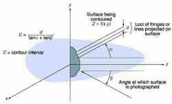
FIGURE 1. Standard shadow interferometry can be used to determine height information. Parameter d is the distance between lines on the grating, and tana and tanb are the angles off the vertical axis for the projector and the camera, respectively. Parameter C is the interval or height change between contour lines. Click here to enlarge image To gain the system resolution required to measure these parameters, many IC inspection systems employ moiré interferometry—an optical technique that uses coherent light to produce a high-contrast, two-beam optical interference pattern. From this interference pattern, the inspection system generates 3-D characteristics of parts such as thin, small-outline packages (TSOPs).Conventional moiré interferometric systems use two gratings to produce interference patterns. One grating is used with a coherent light source, such as a laser, to project a structured image of the part to be inspected. A camera system set up to view these structured lines through a second grating would see a moiré pattern. In shadow moiré interferometry, the shadows projected on a specimen due to one transmittance grating are seen through the same transmittance grating. The beating between two gratings carries the height information of the specimen surface. In conventional interferometric systems, the height or deviation from the ground plane of a particular point on an object under test is defined as z = f (x, y), where z is the height of point f (x, y), and x and y represent the position along the ground plane. Based on this setup, the height can be determined based on the angle of the projector and the viewer and the spacing of the grating (see Fig. 1).
FIGURE 2. SolVision's FalconPro BGA inspection system takes four images of the component and moves the grating slightly for each image. These images are later combined in host memory to create a single moire pattern that contains 3-D position data on the component's shape. Click here to enlarge image While conventional stereovision systems can be used to capture these moiré fringes, they generally work slower than laser-based systems. Laser-scanning systems, on the other hand, are more apt to fail because of the mechanical mirrors that scan the laser light over the part under test. A FAST APPROACHBecause of these limitations, SolVision (Brossard, Quebec, Canada) has developed an optical ball-grid-array (BGA) inspection system, FalconPro IC, that uses fast moiré interferometry. Instead of two gratings, a single grid is moved mechanically four times in front of a collimated light white source, and four separate images of the BGA substrate are captured by a PC-based system (see Fig. 2). After the four images are captured, they are superimposed to create a moiré pattern using a proprietary algorithm developed by SolVision. Another algorithm then converts the phase information in the moiré pattern to calculate the height of each pixel in the combined image.A DCR II white-light source from Schott-Fostec (Auburn, NY) uses a fiberoptic cable to deliver light to a projector designed and built by SolVision with a telecentric lens. This collimated light passes through a glass grating, also designed by SolVision, that creates a pattern of alternating bright and dark lines.
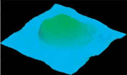
FIGURE 3. SolVision Falcon system can inspection ball and column grid-array packages in addition to PBGA (plastic), CBGA (ceramic), and CSP (chip-scale packaging) types. The 3-D detail is displayed through a proprietary method devised by SolVision. Click here to enlarge image A Hitachi (Simi Valley, CA) KP-F100 1300 x 1030-pixel digital CCD camera captures and transmits an image of the light pattern to the host PC using a Genesis frame grabber from Matrox Imaging (Dorval, Quebec, Canada). After image acquisition, the host directs the frame grabber via an RS-232 cable connection to signal the projector/ grating assembly to move the grating. Grating movements are controlled by a mechanical stage designed and built by SolVision specifically for this purpose. The grating generally moves a fraction of an inch at a time, and this process repeats until four images of the same part with slightly different interference fringe patterns are captured. The entire process takes approximately 150 ms. As a result, the FalconPro system can perform at inspection rates of 60,000 TSOP IC packages per hour.Phase measurements are converted to a 3-D profile and displayed in a 3-D perspective on a 15-in. 151MP flat-panel display from Samsung (Ridgefield Park, NJ; see Fig. 3). Images also can be stored and sent over a SCSI interface to a 9-Gbyte hard drive. Falcon's software offers the option to periodically send archived images via an optional 10/100-Mbit/s EtherJet local-area-network (LAN) card from IBM (Armonk, NY) to remote storage. This LAN also allows remote access to the local drive via semiconductor-manufacturing fabrication protocol standards such as the Generic Equipment Model Standard or the Semiconductor Equipment Communications Standards.If the 3-D profile exceeds certain parameters, such as warpage of substrates, chip-out, peel-off, and grid-to-fiducial offset (reference mark to grid offset) in Falcon's user interface, an action signal is sent via a PCI-based robotic controller card from CyberResearch (Branford, CT) to an S-series pick-and-place clean-room robotic arm from MotoMan (West Carrollton, OH; see Fig. 4). The robotic arm picks those ICs that do not meet acceptable criteria with a vacuum grip and places them in a reject bin.
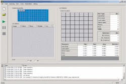
FIGURE 4. FalconPro software offers a selection of IC packaging types that can be checked for defects based on warpage, coplanarity, and other criteria. A self-train technique can teach the system new package types or alter the criteria for the existing library of IC packages.Click here to enlarge image Results by batch, day, or component type are searchable with a user-defined spreadsheet report included in the FalconPro software package. Although the FalconPro software is supplied with the MotoMan pick-and-place arm, SolVision also offers an off-line vision-only system, Falcon, that can be programmed to interface with other programmable logic controllers. SolVision is considering packaging the optical sensor into a more modular format with industry-standard cabling connections for easier integration into other IC-handling systems. Other efforts include expanding the Falcon series of inspection systems to accommodate a larger variety of IC packages by expanding the internal IC packaging specifications library to include newer packaging techniques, such as MicroBGA. COMPANY INFORMATIONAdaptecMilpitas, CA 95035Web: www.adaptec.comCyberResearch
Branford, CT 06405
Web: www.cyberresearch.comHitachi Koki Imaging Solutions
Simi Valley, CA 93063
Web: www.hitachi-hkis.comIBM Corp.
Armonk, NY 10504
Web: www.ibm.comIntel Corp.
Santa Clara, CA 95052
Web: www.intel.comMatrox Imaging
Dorval, Quebec, H9P 2T4 Canada
Web: www.matrox.com/imagingMicrosoft Corp.
Redmond, WA 98052
Web: www.microsoft.comMotoMan
West Carrollton, OH 45449
Web: www.motoman.comSamsung Electronics America
Ridgefield Park, NJ 07660
Web: www.samsung.comSchott-Fostec
Auburn, NY 13021
Web: www.schott-fostec.comSolVision
Brossard, QC, J4W 2V6 Canada
Web: www.solvision.net


