Gate-array-based adaptive computing speeds image processing
Gate-array-based adaptive computing speeds image processing
By Andrew Wilson, Editor at Large
For executing demanding computational tasks such as image-processing, hardwired functions prove more efficient than applying general-purpose microprocessors. For this reason, Adaptive Computing Systems (ACS) of the Defense Advanced Research Projects Agency (DARPA; Arlington, VA), among others, is promoting the use of reconfigurable computing in military-imaging systems. Once deployed, such adaptive computing systems are expected to easily extend and upgrade many imaging systems.
The development of these systems requires field-programmable gate arrays (FPGAs) and FPGA-based hardware with sufficiently fast configuration times and sophisticated high-level software-development tools that can take advantage of the underlying hardware. Already, several university and commercial projects are heavily involved in solving problems with reconfigurable computing related mainly to military image-processing applications such as pattern matching and automatic target recognition.
With the advent of the FPGA, system designers found that much of the glue logic required on printed-circuit boards (PCBs) could be incorporated into single devices, saving both real estate and manufacturing costs. As the functionality of these devices increased, designers realized they could off-load specific functions from the microprocessor, effectively hard-wiring them and increasing their speed.
To build such image-processing systems, some researchers and manufacturers are looking to combine reduced instruction set computer (RISC) cores with FPGA devices. For example, at National Semiconductor (Santa Clara, CA) and the University of California (Irvine and Berkeley, CA), work is underway to develop reconfigurable processors.
Under a DARPA contract, National has developed its adaptive-processing architectural NAPA1000 processor, a single integrated circuit (IC) that combines scalar, reconfigurable, and parallel computing. To provide these functions, National engineers have integrated a 32-bit RISC processor core and peripherals, a 50,000-gate adaptive logic processor, and 16 kbytes of data memory onto a single die.
According to National`s Tim Garverick, the on-chip FPGA serves as a dynamically reconfigurable computing resource that allows algorithms to be accelerated through gate-level customization. Using an on-chip SRAM, developers can define the functionality of the FPGA array by completely rewriting it in 100 ms under the control of the RISC processor.
"In a typical application, such as feature extraction or image formation, the RISC processor supports control of "outer-loop" functions, while the FPGA speeds "inner-loop" performance," says Garverick. To develop such applications, Garverick foresees applications being first compiled to run on the RISC processor and performance critical loops migrated to the FPGA as the development process proceeds.
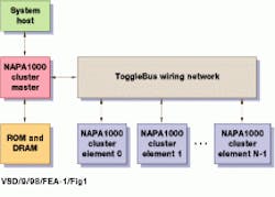
To provide linear performance scaling for common signal-processing algorithms without the need for external crossbar switches, National has incorporated an on-chip ToggleBus wiring network. "This allows the device to the used in parallel-processing arrays of up to 1024 elements to realize systems with teraflops performance," says Garverick (see Fig. 1). Already, the company is discussing cooperative development projects with other semiconductor vendors to establish standards in the adaptive computing systems area.
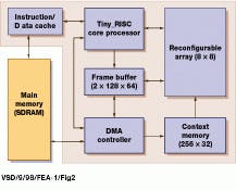
Like National, re searchers at the University of California, Irvine, and at Obsidian Technology (Laguna Niguel, CA) are exploring the use of combining RISC and programmable processing elements in an IC. Dubbed MorphoSys, the IC is composed of a reconfigurable array, a control processor, a data buffer, and a DMA controller (see Fig. 2).
It targets image-processing applications using a 32-bit RISC core processor called Tiny RISC, which controls the operation of rows of reconfigurable blocks that resemble rows of coarse-grain reconfigurable blocks. Note that these blocks are unlike the fine-grain blocks of the 4000 series FPGAs from Xilinx (San Jose, CA). In operation, the Tiny RISC processor loads configuration data from main memory into context memory through a DMA controller. After the frame buffer is loaded with image data from main memory, Tiny RISC issues instructions to the reconfigurable array for execution.
According to Robert Heaton, chief executive officer of Obsidian Technology, this makes the MorphoSys processor ideal for applications such as automatic target recognition, where synthetic-array-radar search data can relate to the coverage of 40,000 square nautical miles to a resolution of 1 m. "If the targets in such image data are partially obscured," says Heaton, "computational levels reach the hundreds of teraflops range, and it is obvious that a hardware approach is required."
Target recognition
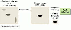
One target-recognition approach thresholds regions of interest (ROI) to generate binary images that are then matched to binary template targets (see Fig. 3). Using the MorphoSys processor, a template of 8 ¥ 8 pixels, which represents the ROI, is first loaded into the reconfigurable array and compared with a threshold value. After this comparison, a 128 ¥ 128 binary image is generated and stored in the frame buffer. This binary image is then matched against the target template to perform the automatic target-recognition function.
"For 16 pairs of target templates," says Heaton, "processing time is about 16 ms with an IC clock speed of 100 MHz. This processing is approximately one order of magnitude faster than a comparable system using Xilinx XC4010 FPGAs."
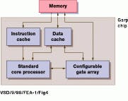
"Traditional FPGAs lack a reasonable computing and usage model to make application development portable across platforms and generations," says John Wawrzynek of the Computer Science Division of the University of Berkeley. According to Wawrzynek, it is notoriously difficult to map computations efficiently to FPGAs. As a result, Wawrzynek`s group, the Berkeley Reconfigurable Architectures, Systems and Software (BRASS) group, is also developing a combined RISC and reconfigurable gate array on a single piece of silicon. Known as Garp, the first implementation of the IC combines a single-issue MIPs core with a gate array or ganized as 32 rows by 23 columns (see Fig. 4).
To ease application development using the device, Wawrzynek and his colleagues are defining an application binary interface (ABI) for the chip that serves as the interface be tween applications and the system, where the system in cludes both the detailed device architecture and the primitive run-time software. "The advantage of defining an ABI is to provide computing platforms that allow third-party software development and the preservation of software while developing new implementations," Wawrzynek says. He envisions a basic set of generators for common arithmetic functions such as addition and multiplication and a more specialized set for DSP operations such as finite impulse response filters or fast Fourier transforms (FFTs).
Host CPUs
While many researchers are finding ways to combine RISC cores with programmable logic, others are using standard PCs or workstations coupled to reconfigurable computing platforms. In addition to focusing on target recognition applications, researchers are porting other image-processing functions, such as Fourier analysis and morphing, to such designs.
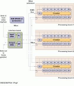
For example, at the Bradley Depart ment of Electrical Engineering of the Virginia Polytechnic Institute and State University (Blacksburg, VA), Peter Athanas and his colleagues have implemented a two-dimensional (2-D) FFT on the Splash-2, a second-generation reconfigurable attached processor designed by the Supercomputing Research Center (Bowie, MD). Consisting of a Sun Microsystems Sparc-2 host, an interface board, and one or more array boards, the architecture can support up to 15 Splash-2 array boards, each containing 17 Xilinx XC4010 FPGAs arranged in a linear array and fully connected through a 16 ¥ 16 crossbar (see Fig. 5).
To implement an FFT on the Splash-2 architecture, floating-point arithmetic add/subtract and multiplier units are used. "Until recently," says Athanas, "any meaningful floating-point arithmetic has been virtually impossible to implement on FPGA-based systems due to the limited density, routing resources, and speed of older FPGAs." Now, with the introduction of very-high-speed IC hardware-description language, rapid prototyping makes such structures easier to develop.
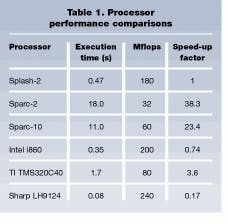
To evaluate the performance of the FPGA approach, Athanas compared the results of performing a 512 ¥ 512 2-D FFT, a 512 ¥ 512-point multiplication, and a 512 ¥ 512 2-D inverse fast Fourier transform on several different architectures (see Table 1). Although the Splash-2 performs more than a magnitude better than a general-purpose computation, its performance is similar to an implementation of the algorithm run on an Intel i860 processor board. Interestingly, the FPGA implementation runs just six times slower than the LH9124 processor from Sharp Microelectronics Technology (Camas, WA), one of the fastest hardwired FFT processors available (see "FFT chips quicken image recognition systems in vision systems," Vision Systems Design, August 1998, p. 36).
Off-the-shelf products
Commercializing reconfigurable computing has been the aim of a handful of companies, including Giga Operations (Berkeley, CA), Annapolis Micro Systems (Annapolis, MD), Embedded Solutions (Wokingham, Berkshire, England), and VisiCom (San Diego, CA).
As the largest and most powerful member of the Wildfire family of reconfigurable computing boards, the Wildfire array card from Annapolis Micro Systems contains 16 Xilinx XC4044XL parallel processing elements and one control processing element. In the implementation of a Prewitt image-filtering operation, such systems have operated more than 160 times faster than using a Texas Instruments TMS320C5x digital-signal processor (see "Field-programmable gate arrays boost imaging performance," Vision Systems Design, Feb. 1997, p. 38).
Also implemented with Xilinx gate arrays, the G900 PCI-32 reconfigurable interface card from Giga Operations provides host bus, peripheral input/output (I/O), and four module (MOD) sockets. Up to 16 of the company`s XMOD processing, data routing, and I/O cards can be plugged into MOD sockets as four stacks of four.
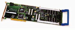
Alpha Data Parallel Systems (Edinburgh, Scotland) and Embedded Solutions are also offering a PCI-based reconfigurable computing board (see Fig. 6). Known as the RC1000-PP, the board can be populated with either Xilinx XC4085XL or XC40125XV FPGA devices. Jointly developed by the two companies, the board is aimed at image-processing and digital signal-processing functions, according to Roger Gook, managing director of Embedded Solutions. Benchmarks on several image-processing functions have already been developed under the company`s Handel-C hardware compilation toolset (see Table 2).
"Handel-C is a software tool that translates source code describing the circuit into a net-list--the file that specifies logic gates and the connections between them," says Gook. "This reduces the design time of complex circuits and enables software reuse in hardware for application acceleration," he adds.
Application acceleration was of primary concern to the developers of the Falcon board from VisiCom (San Diego, CA). As a combined frame grabber/ image processor/display controller, this PCI-based board implements FPGA devices to perform reconfigurable image-processing functions (see "Choosing a PCI-based frame grabber for vision applications," Vision Systems Design, August, p. 46).
The board has already been implemented as part of the Model 66Z x-ray inspection system from American Science and Engineering (AS&E; Billerica, MA). Engineers at AS&E chose the board because edge-enhancement and zoom features could easily be incorporated and upgraded into the system (see "Reconfigurable image processors tackle bomb-inspection tasks," Vision Systems Design, Feb. 1997, p. 42).
Microscope vendor JEOL (Peabody, MA) has chosen the board as part of its Xvision Plus option for the company`s electron-scanning microscopes. "One of the requirements for the Vision Plus was that it had to support recursive frame averaging," says John Smith, VisiCom principal engineer. "This process removes noise and creates a sharper image. As a result, JEOL could produce a true 1k ¥ 1k recursive averaged image," he says.
While the benefits of adaptive computing systems include system reconfigurability and high-speed image processing, FPGA-based image processors have yet to be used extensively in commercially available vision systems. The major reasons are that FPGA-systems remain specialized, and easy-to-use image-processing libraries that can reconfigure FPGAs are not readily available. However, the push by DARPA and others for such image-processing systems will eventually lead to the development of such systems. When this happens, adaptive computer systems will fulfill the promise of reconfigurable computing.
FIGURE 1. Under a DARPA contract, National Semiconductor has developed a NAPA1000 adaptive-processing architectural processor. This single integrated circuit combines scalar, reconfigurable, and parallel computing using a 32-bit RISC processor core and peripherals, a 50,000-gate adaptive logic processor, and 16 kbytes of SRAM data memory. To provide linear-performance scaling for common signal-processing algorithms without the need for external crossbar switches, the IC incorporates an on-chip ToggleBus wiring network to structure parallel-processing arrays of up to 1024 elements.
FIGURE 2. Researchers at the University of California have combined RISC and programmable processing elements into a MorphoSys integrated circuit for handling target image-processing applications. Containing a reconfigurable 8 ¥ 8 array, a Tiny RISC core processor, a 2 ¥ 128 ¥ 64 frame buffer, a DMA controller, a 256 ¥ 32 context memory, and an instruction/data cache, this IC loads configuration data from main memory into context memory through the DMA controller. After the frame buffer is loaded with image data from main memory, the Tiny RISC processor issues instructions to the reconfigurable array for execution.
FIGURE 3. Target recognition can be performed by thresholding regions of interest (ROI) in an image to generate binary images that are then matched to binary template targets. Using the MorphoSys processor, a binary template of 8 ¥ 8 pixels, which represents the ROI, is first loaded into the reconfigurable array and compared with a threshold value. After this comparison, a 128 ¥ 128 binary image is generated and stored in the frame buffer. This binary image is then matched against the target template to perform the automatic target-recognition function.
FIGURE 4. Because it is difficult to map computations efficiently to FPGAs, the Berkeley Reconfigurable Architectures, Systems and Software group is developing a combined RISC and reconfigurable gate array on a single piece of silicon. Called the Garp chip, the first implementation of the IC combines a single-issue MIPs core processor, instruction and data caches, and a configurable gate array organized as 32 rows by 23 columns.
FIGURE 5. At the Bradley Department of Electrical Engineering of the Virginia Polytechnic Institute and State University (Blacksburg, VA), researchers have implemented a two-dimensional fast Fourier transform on the Splash-2, a second-generation reconfigurable attached processor designed by the Supercomputing Research Center (Bowie, MD). Consisting of a Sun Microsystems Sparc-2 host, an interface board, and one or more array boards, the architecture can support up to 15 Splash-2 array boards, each containing 17 Xilinx XC4010 FPGAs arranged in a linear array and fully connected through a 16 ¥ 16 crossbar.
FIGURE 6. Alpha Data Parallel Systems and Embedded Solutions are providing a PCI-based reconfigurable computing RC1000-PP board. It can be populated with either Xilinx XC4085XL or XC40125XV FPGA devices. Jointly developed by the two companies, the board suits image-processing and digital signal-processing functions.
Supporting increasingly complex computational systems usually results in the need to handle ever-greater data-flow bottlenecks. This need is particularly true of image-processing environments, in which high-end applications frequently demand short bursts of high performance that typically require either multiprocessor or hardwired architectural approaches. Among the variety of microprocessors available to imaging-system designers, general-purpose digital-signal processors (DSPs), such as the TMS320C40 series from Texas Instruments (Dallas, TX), are generally used. However, in many imaging applications, the required processing throughput of such processors often falls short of real-time operations.
For example, a demanding application required the support of a system that had to filter 16-bit resolution data accumulated from 256 channels at 36 kHz. Spectrum Signal Processing (Burnaby, Quebec, Canada) was called on to produce this system, which also called for each channel to be processed through a 128-tap finite impulse response (FIR) filter. In addition, 16-bit tap weights and a total system throughput of 1.18 Gtaps/s were also required.
Due to the low volume involved, a hardwired approach was deemed infeasible. Moreover, a multi-DSP architecture--implementing between 40 to 80 TMS320C40 DSPs--was also ruled out as being too costly. As a result, Spectrum approached MiroTech Microsystems (St-Laurent, Quebec, Canada) to resolve this computational challenge with one of its reconfigurable computing architectures.
Using two 60-MHz TMS320C40 DSPs and two MiroTech HPRC X-C436 series modules, an imaging-processing system was configured so that one C40 DSP was assigned the task of deinterlacing 256 multiplexed channels and shipping data in packets of 889 pixels to the field-programmable gate array (FPGA) based (X-C436) processing pipes. At the output, the other C40 DSP reassembled the data stream. Packetizing data in 889 pixels allowed filter re-initialization when switching channels and maintained an 86% pipe-processing efficiency. Every pipe was implemented in one of the two Xilinx XC4036 FPGAs available on MiroTech`s X-C436 module.
The filters, implemented in bit-serial distributed arithmetic, needed 18 cycles to process 16-bit resolution data and weight coefficients. At 50 MHz, each filtering pipe was processing 2.8 million samples per second or 358 Mtaps/s, providing a throughput of 1.4 Gtaps/s. At the internal FIR rate of 86% efficiency, the maximum throughput was 1.204 Gtaps/s, which exceeded the 1.18 Gtaps/s requirement.
Pierre Popovic
President
MicroTech Microsystems
St-Laurent, Quebec, Canada
