Fast Semiconductor Inspection with High-Resolution Color Line Scan Cameras

Klaus Riemer, Project Manager for Chromasens GMbH
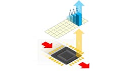
Semiconductor geometries and printed circuit board (PCB) components are becoming increasingly smaller, while the demands on quality testing and control are growing. To meet these demands, modern color line scan cameras can enhance and expand the industry’s inspection capabilities.
Because of the minute structures involved, optical inspection in modern semiconductor manufacturing now occurs in the micrometer range. The need to detect defects and contaminations at this scale places the highest demands on inspection systems. Extremely high-resolution color line scan cameras with CMOS technology can capture these minute structures at high speeds for image analysis.
Furthermore, miniaturization does not stop at printed PCBs, with several PCBs now being produced on a single panel to increase efficiency. These components must also undergo 100% inspection with high throughput.
Color Line Scan Cameras with CMOS Technology
Line scan cameras are suitable for image-capturing tasks where fast-moving large areas or flat objects must be captured and analyzed with high optical resolution.
In a CCD line scan camera, the light-sensitive pixels of the CCD line scan sensor are arranged in a single line, and they are read out according to a CCD sensor’s operation. The readout cycle is adapted to the throughput speed of the inspected objects or surface areas. The whole two-dimensional image is then created by joining the individual lines together. The generated image is almost distortion-free because of the line-by-line scanning in time with the object transport and in the transport direction.
CCD sensors have long been the technology of choice in line scan imaging because of their image quality, high sensitivity, low noise, low Photo-Response Non-Uniformity (PRNU), high dynamic range, and signal-to-noise ratio. These benefits are essential in line scan because of the high-speed image acquisition and reduced number of photosensitive cells, which means exposure is limited in time and intensity.
New generation CMOS line scan sensors now offer a similar image quality as CCDs, coupled with additional benefits specific to CMOS technology such as higher readout speed and flexible readout modes. Unlike single-line CCDs, these sensors have several lines of pixels, allowing for different operation modes depending on an application’s requirements. One key benefit of a multiline sensor is the time delay integration (TDI) option. TDI consists of adding up the values of adjacent pixel lines synchronously with the motion of the object below the camera. The same section of the object is imaged by several lines, and adding up the signals of all these lines increases the signal intensity compared with a single line sensor. This solution has a much better signal-to-noise ratio than an equal increase in gain.
The combination of specially adapted line illumination with these high-performance line scan cameras results in a powerful overall system that is optimally matched to the application. The illumination system homogeneously illuminates a line on the object with a very high luminosity whereby the light color and the illumination geometry can be precisely and variably adapted to the image capture requirements.
Solutions for Semiconductor and PCB Production
Profitability in semiconductor manufacturing relies on the level of flawless product yield. Therefore, manufacturers test their products multiple times, starting with the bare wafers and ending with inserting the chips into the IC packages.
As the wafer moves along the production line, more components are placed on it, thereby increasing its complexity. Yield-reducing defects must, therefore, be identified as quickly and as early as possible while also reducing the overall inspection time. This results in more inspection points at each process step in the production line, with the inspection system required to produce the scan results more quickly. Inspection throughput is critical to the fab’s overall production.
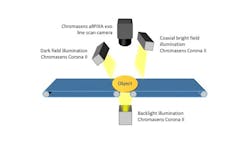
Scanning and illumination techniques offer a solution by providing faster and more efficient semiconductor inspection. As a rule, wafer inspection is performed with dark-field illumination and coaxial bright-field illumination. PCBs can be inspected using a combination of diffuse light and bright-field illumination—the diffuse light is used primarily for 3D-shaped components to eliminate gloss and reflections while the bright-field lighting is used to inspect the substrate itself (Figure 2).
New generation cameras feature multichannel illumination functionalities that make it possible to use different types of illumination in one single scan. Acquiring up to four different images in one scan provides much more information and improves defect detection. In addition, those cameras provide multifield imaging to generate HDR images from up to four lines captured with different settings. This allows object details to be detected in both bright and dark areas in the image. Both features can be combined to increase the detection reliability and shorten the inspection time.
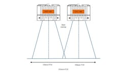
The trend toward miniaturization continues for PCBs and the components mounted on them. This leads to so-called panelization whereby several PCBs are manufactured on one panel. Each printed circuit board on the panel is subsequently identified by a unique barcode, and thus rapidly inspecting the printed circuit boards is correspondingly complex and demanding. For example, during the visual inspection, existing solder defects, such as interruptions, solder bridges, solder short circuits, or excess solder, must be identified in addition to component defects like lifted solder and missing or misplaced components. A color line scan camera system can perform these inspection tasks with great accuracy because of its high operating speed and lateral resolution. (Figure 3)
Oxidized copper wires on PCBs must also be detected, yet monochrome systems cannot reliably identify oxidized areas. However, high-performance color line scan cameras such as the allPIXA evo, combined with high-performance illumination, excel at this task.
Optimized lighting is also indispensable for reliable and precise inspection results in printed circuit board inspection. For example, the reduced shadows and homogeneity of tunnel lighting ensure very high image quality, meaning fewer defects are overlooked. Where coaxial illumination is required, it can be configured with white light or a specific wavelength.
Application examples from semiconductor and PCB manufacturing illustrate that high-performance color line scan cameras can play an important role as central components in 100% real-time inspection processes. The image quality and resolution performance of multiline full-color CMOS line sensors result in a particularly high application potential for camera systems. Fast and accurate color measurements and rapid 3D inspection are additional future applications for color line scan cameras in this performance class.