Advanced Assembly Techniques for Imaging Lenses

As camera technology keeps advancing, the applications for imaging systems continue to get more and more demanding. Images have more and more information that needs to be collected as cameras add more and more pixels. To do this, the pixels are getting smaller, and sensors are getting larger to fit more pixels on them. Both of these result in it being more difficult for lenses to keep up with camera performance.
Drop-Together Assemblies
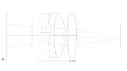
The vast majority of machine vision lenses, or the lenses designed to go onto industrial and scientific cameras to capture images a computer can make decisions from, are constructed in a method called "drop together." This method consists of precision machined barrels, spacers, and optics being assembled together and held in place with retainers. The mechanical tolerances on the fits of the lenses’ outer diameters to the metal’s inner diameter, along with other mechanical tolerances, are what define the precise position of all the optical surfaces. This method requires tightly-controlled mechanical tolerances on both glass and metal. These optical tolerances often seem daunting to mechanical engineers from other industries with diameters, concentricities, and thicknesses controlled on the order of 10 µm.
The Need for Advanced Assembly Techniques
Precision optical assemblies needed for machine vision typically require the location of optical surfaces to be controlled anywhere from 10 to 50 µm from their nominal position. As the required performance continues to increase, the precision of optical surface placement continues to get more demanding as well.
If a lens is decentered or moved way from the optical axis of the system by even several µm, it will change the angle that each ray strikes the curved surface of the lens. Changing this, in turn, changes how much the ray is bent as it passes through the surface. All these changes will result in rays striking the sensor at different locations, with some rays from one object point falling on different pixels than other rays from the same object point. This results in image blur and loss of contrast.
As pixels get smaller, the allowable error in the location of each ray on the image plane gets smaller and more difficult to achieve. The sensitivity to the positional errors on the lens surfaces described above also increases. Larger pixels are more tolerant to small errors than smaller pixels.
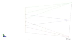
Another more complicated factor requiring increased assembly precision is that as sensors get larger, even if the pixels stay the same size, the sensitivity to these errors also increases significantly. This is for many reasons, but the primary cause and simplest one to illustrate is related to angles. One of the results in the errors in the position of the optical surfaces is something called beam pointing. When a lens surface is decentered or positioned in such a way that the center of the lens’s curvature is moved away from the center of the barrel (the z-axis), it results in the light going through the lens to be bent away from the z-axis. This beam pointing will result in the image formed by the lens being tilted and not perfectly perpendicular to the z-axis anymore. In addition to the alignment of the optical surfaces being a source of error, the actual tilt of the camera’s sensor relative to the mounting feature of the lens is also a source of image tilt (Figure 2). Both of these sources are generally rather small on the order of several arc minutes. But as the sensor sizes increase, a small angle starts to result in larger displacements of the sensor from the ideal image plane. Therefore, the edges or corners of the image are further or closer than the ideal focus even when the center is perfectly focused, resulting in a defocus or blurring of the edges and corners.
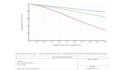
To illustrate the effects of this tilt we can look at a popular chip size from several years ago, the 1/1.8” format and compare it to the new Sony Pregius IMX530 and look how the same amount of image plane tilt can affect the image. A 1/1.8” sensor has a 9-mm diagonal, which means the corner is 4.5 mm away from the center of the chip. For the IMX530, the diagonal dimension is 19.3 mm, meaning that the corner is 9.65 mm from the center. If a sensor is perfectly focused in the center, a 5 arc minute tilt would cause the corner of a 1/1.8” sensor to be about 6.5 µm out of focus, and on the IMX530 it would be greater than 14 µm out of focus. These are very small values, but 14 µm of defocus can have a dramatic difference in image quality on even a relatively fast lens. Figure 3 shows the modulation transfer function (MTF) for a paraxial (perfect) lens with an image plane tilted by 5 arc minutes. The blue line is the center of the image and is in perfect focus, the green line is at the corner of a 1/1.8” chip, and the MTF drops about 10 contrast points at 145 lp/mm, while the red line, which is the corner of an IMX530, drops about 50 contrast points.
The Solution: Active Alignment
To increase performance of the system further to keep up with the smaller pixels and larger sensors, different assembly techniques are required. These techniques are not necessarily new, as most have been used in other industries and products, but are largely new to the machine vision market. Some of these techniques have long been used in microscopy, astronomy, and other industries where the expense of the added skilled labor was acceptable. High volume consumer electronics have also used similar techniques but with automation and robots that greatly reduce the assembly cost but require large volumes to amortize the setup expense.
These assembly techniques are often called active alignment or active compensation. Where the position, in x, y, and z coordinates, and angular tilts of all the optical surfaces are either aligned to a common axis, or some of the optical surfaces are adjusted while getting performance feedback to optimize the performance (Figure 4).
Both techniques require precision testing either of the location of the surfaces or of a performance metric such as MTF or transmitted wavefront error. They require either a skilled technician to do the adjusting or precision robotics in an automated system. Once the surface or surfaces are in the optimal position, they also require a way to be fixed in place ruggedly enough to remain in place throughout the operation of the camera system. This is typically done with adhesives, but other mechanical methods are also possible. Using adhesives increases the assembly time considerably over a traditional drop together and retained system. This added assembly time is both assembler/machine time with the added gluing operation and also wait time during the adhesive curing process, during which the assembly is usually kept in a fixture while the adhesives are cured.
The correction of one or more optical components while optimizing for overall performance can involve the location of lens elements, or it could be the position of the sensor itself. Actively tilting the sensor while optimizing performance can address both the beam pointing errors and the mechanical tilt errors inherent between the camera and lens interface.
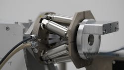
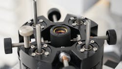
Positioning the optical surfaces accurately also requires the ability to move the optics very small distances accurately and holding them there precisely while the lens is fixed in place. This typically requires special fixturing and fine motion controls. Advances in robotics and motion controls have made this easier and less expensive to implement, opening more opportunities to the automation of assembly processes (Figure 5).
These techniques do require special attention during the design of the optics, to really take full advantage of them. To get the most out of the lens system, it needs to be designed with the assembly technique in mind. Just taking a design optimized for drop-together assembly will likely not end up with as high performance as a lens specifically optimized to get the most out of the active correction, even if both are assembled with the same techniques.
These advanced assembly techniques are opening up new level of performance to the machine vision camera market, but they require more engineering effort in the design and execution of the lens assemblies. This will add cost and time to the lens development but can achieve new levels of performance. As sensor technology continues to drive performance further and further, these techniques will need to be more common place in lens design and assembly.
About the Author
Jeremy Govier
Jeremy Govier is senior principal engineer at Edmund Optics, Barrington, NJ, USA.