IMAGE SENSORS: Black silicon sensors target low-light level, IR imaging

Although CMOS-based imagers are now commonplace in many of today's solid-state cameras, the very nature of the silicon material they are built from limits their spectral response. At both short and long wavelengths, the quantum efficiency (QE) of standard CMOS imagers is drastically reduced, making them unsuitable for application in the UV and SWIR spectrum. However, by applying specialized semiconductor processing methods, the QE of such devices can be improved.
To image the UV spectrum, for example, techniques such as backside-illuminated sensors in which incident photons are collected on the backside of the sensor. Other more sophisticated techniques use Boron doping in conjunction with backside illumination to increase the QE of CMOS sensors at UV wavelengths. Indeed, this is the method used by Alacron (Nashua, NH; www.alacron.com) in the design of its FC-300 UV camera.
To increase the QE of such imagers in the NIR spectrum, companies such as SiOnyx (Beverly, MA; http://sionyx.com) are developing CMOS imagers that also employ novel semiconductor fabrication methods. Emerging from the work of Professor Eric Mazur of Harvard University (Cambridge, MA, USA; www.harvard.edu) over a decade ago, the process used by SiOnyx irradiates off-the-shelf silicon with a series of laser pulses in an atmosphere sulfur hexafluoride.
During this process, laser energy melts and re-solidifies the top surface of the silicon wafer, trapping quantities of sulfur from sulfur hexafluoride gas in the solid material, thus doping the semiconductor with sulfur impurities. In addition, the physical surface of the silicon is transformed from a smooth shiny wafer into a surface of microscopic spikes. Both these effects increase the spectral sensitivity of the silicon.
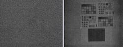
Wafers processed in this manner can be used to fabricate imagers that are more sensitive to IR light than standard CMOS imagers. At this year's SPIE Defense and Security Symposium in Baltimore, MD, SiOnyx showed three such imagers based on the technology. The company's XQE family includes the XQE-1310, a 1in imager with 1280 x 1024 10 µm pixels, the XQE-0920, a 1/2in format imager with 1280 x 1024 5.6 x 5.6 µm pixels and the XQE-0570, a 1/3in format imager with 872 x 654 5.6 x 5.6 µm pixels.
According to Dr. Martin Pralle, Vice President of Business Development with SiOnyx, all the XQE sensors feature a 72dB native dynamic range and an on-chip high dynamic range feature that allows up to 120dB dynamic range to be achieved.
To date, the company has not yet published the spectral characteristics of these devices but, Pralle says, these will be available to potential customers willing to sign an NDA agreement. All Pralle would say was that at approximately 1064nm, the devices exhibited a QE approximately ten times that of standard CMOS image sensors. For night-vision applications, the US Army recently tested the SiOnyx XQE-1310 sensor in its labs and confirmed imaging at 1 mLux (1×10-4 Ft-candles).
To evaluate the sensors, the company has also introduced a range of prototype cameras Ethernet-based cameras that incorporate TI's DM368 DSP. This can be used for real-time H.264 motion compression, a feature useful in surveillance applications where image data may need to be transmitted over Ethernet-based networks. The company will also tailor specialized image sensors, camera modules and cameras depending on the requirements of particular markets.
Vision Systems Articles Archives