Researchers use to store image data
Researchers use to store image data
By Richard Parker, Contributing Editor
ser demands for storage of movies, multimedia archives, and entire databases of hospitals, law firms, government agencies, and libraries containing hundreds and thousands of terabytes have not resulted in ideal storage solutions. Instead, such demands have spawned large and bulky robotically controlled CD jukeboxes. Consequently, renewed research in all-optical memory technologies aims to store massive amounts of information inexpensively on small-sized media.
Images and data are now generally written and accessed to and from optical memories by a laser. Usually, the optical recording medium is a photorefractive or photosensitive material that uses holographic techniques to store informa-
tion. Other all-optical techniques that rely on photon interaction are also under investigation.
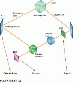
Holographic-type memory devices are close to commercial reality. Such holographic memories record both the intensity and direction of a light beam from a spatial light modulator (SLM) on a storage material--the beam represents the input data, and the SLM formats the data on the photosensitive material.
A second beam, known as a reference beam, is reflected by a rotating mirror at a specific angle onto the photosensitive material. Interaction of the two beams forms an interference pattern that is recorded in the storage material. When the reference beam is again directed at exactly the same angle, the stored pattern or page is recalled. Changing the angle of the reference beam by a fraction of a degree makes possible the storage and retrieval of different information. The information is generally read out by a solid-state camera (see Fig. 1).
Common optical storage materials being used in such systems are photorefractive materials like lithium-niobate crystals doped with traces of iron. Other work is also ongoing using cerium-doped lithium niobate crystals and photoreflective materials such as thin-film polymer. Whereas these materials may prove less expensive and thinner than doped lithium niobate crystals, they require more surface area to store a given amount of information.
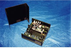
Although most holographic memories are still in development, some are currently available. In August 1995, Holoplex (Pasadena, CA) introduced the HM-100 claiming it as the first commercially available holographic memory. The memory can hold up to 1000, 8-bit, 640 ¥ 480-pixel gray-scale images and can access them in 1 s. The 8 ¥ 8 ¥ 3 5/8-inch module provides a parallel optical or video output. Thanks to its high-speed access capability, it is being used by Hamamatsu (Japan) as a holographic lock that can store as many as 1000 fingerprint images for secure entry access.
"The HM-100 can double as a holographic correlator. Reconfigured as the HC2002, it is being used by Sony (Japan) for gesture recognition in interactive video games," says Holoplex`s chief engineer Yon Quao (see Fig. 2).
Signal to noise
Bert Hesselink, founder and chief technology officer for Optitek (Mountain View, CA), emphasizes that Holoplex`s holographic memory is an analog device with a lower signal-to-noise ratio (S/N) than a digital approach. All holographic memories suffer from low S/Ns, a situation that is exacerbated by the use of low-level signals, crosstalk, high-speed response times, high-rate throughputs, and large amounts of data. As a result, for applications such as fingerprint storage and retrieval, system requirements demand analog holographic approaches.
Optitek is developing a digital holographic memory with bit-error rates (BERs) of 10-12 to 10-14, compared to analog devices that provide BERs of 10-3 to 10-4. "Although we are about two years away from commercializing such a product, it will provide storage densities of several hundred bits per square micron and data-transfer rates of 10 to 100 Mbytes/s," says Hesselink,
Hesselink, a researcher at Stanford University (Palo Alto, CA), has demonstrated a digital holographic storage system with 163 kbytes of storage and a data-transfer rate of 63 Mbyte/s. He believes such a development proves that digital optical memory can be commercialized. Hesselink, the principal investigator on two collaborative efforts being funded by DARPA and the National Storage Industry Consortium, is also investigating photorefractive storage materials and holographic data-storage systems. The effort involves several leading companies, including IBM.
At the IBM Almaden Research Center (San Jose, CA), Hans Coufal has demonstrated a system able to store up to 200 holograms composed of 37.5-kbyte pages of 640 ¥ 480 pixels in a crystal less than 1 cm to a side for a storage density of 48 Mbyte/cm3. These results are far short of the goal of a practical storage density of 10 Gbyte/cm3.
According to IBM, such developments do illustrate that progress continues to be made in lasers, SLMs, CCD detector arrays, and light deflectors. This hardware is expected to lead to a cost-effective and practical digital holographic storage system 2003. The demonstration that occupies a footprint of 18 ¥ 24 in. (excluding a 530-nm argon-ion laser), is called the DEMON (digital holographic demonstrator).
Four dimensions
Another holography approach, four-dimensional (spectral) holography via spectral-hole burning, is being championed by Templex (Eugene, OR) as the solution for the needs of next-generation optical storage. The core technology of TASM (temporarily accessed spectral multiplexing) was developed by Templex`s chief technology officer Thomas Mossberg, who was previously affiliated with Harvard University (Cambridge, MA) and then at the University of Oregon (Eugene, OR). He has been granted four patents for optical-storage and communications applications based on his work.
Templex`s research shows that when using TASM, cryogenically cooled YAG crystals doped with frequency-selective ions of the rare-earth element thulium can provided optical storage densities to 100 Gbit/in.2 at microsecond access times. In fact, Templex has demonstrated what it claims is the highest storage density-I/O product term known for an optical storage device--1.5 ¥ 1017 bits/in.2/s--while storing more than 8 Gbit/in.2
Unlike standard holographic memories, which are massively parallel output devices, TASM operates in a serial mode. This mode makes it compatible with most computer configurations. The technique is being used on what the company calls an optical DRAM or ODRAM (see Fig. 3). Key to its operation is the fact that the recording medium absorbs different amounts of light from an input laser beam depending on the beam`s frequency (color), a characteristic that can be controlled. ©
In the ODRAM, an input laser beam is fed into a modulator and then encoded electronically with data supplied from a high-speed data bus. The encoded beam then encounters a beam deflector that feeds the data onto various discrete spots for storage in the memory`s crystal chamber. Stored data are recalled in the form of another encoded optical beam. A detector converts the optically encoded signal to an electronically encoded one. The high-speed data bus then receives the electronic data signal from the ODRAM.
Two-photon effect
Instead of hologram technology, researchers at Call/Recall (San Diego, CA) are developing an experimental ROM prototype that allows writing and accessing of information in a three-dimensional (3-D) volume by using a two-photon effect. In this approach, information is stored in polymer matrices, where it can be accessed in a bit-by-bit or two-dimensional (2-D) multibit-plane format. Readout 3-D systems have also been built.
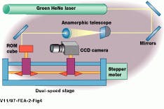
The writing process is based on two laser pulses, which are adjusted so that either pulse by itself does not have enough energy to write a bit. However, the two together can bump the energy level of an active dye molecule into an altered optical state (see Fig. 4). This operation allows the memory system to place a bit in a specific location inside the polymer.
To write terabits of information, information is piped to a liquid-crystal shutter, and light from one of the two lasers is passed through the shutter. With the polymer illuminated uniformly by the second laser, a pattern of bits on the shutter is impressed onto the dye molecules via the AND logical operation. Each such write operation produces a 2-D slice in the 3-D optical medium. The chemistry of the dye systems is structured so that the operation produces a permanent chemical change that alters the polymer`s optical properties. Essentially, the dye molecules change their configuration.
Altered dye molecules are sensitive to a specific wavelength of red light. This characteristic allows a read operation to take place by passing laser light through the storage cube at the key wavelength. Anywhere a written bit exists, the dye molecules fluoresce, and the pattern of bits can be recorded by a CCD imager. Ideally, for one molecule, only two photons are needed to store one bit of information, thus the term "two-photon effect." Accordingly, memory systems holding 100 terabits of data could be conceivably built in a very small volume.
All-optical storage techniques currently under investigation lack the key system components needed to make them viable, namely high-bandwidth high-capacity spatial light modulators for data input, optimized sensor arrays for data output, and high-power low-cost lasers. In addition, optimal multiplexing schemes, access modes, data encoding/decoding, and signal-processing methods must be achieved. Nevertheless, because sufficient progress is being made in all these areas, many mass-storage memory experts foresee commercially available all-optical systems by the turn of the century.
FIGURE 1. In a digital holographic storage system, data to be stored are formatted into a page of pixels by a spatial light modulator (SLM). For each page of information, the rotating mirror changes the angle of the reference beam. The object and reference beams interfere in the storage material to record the data. During readout, the reference beam is directed by the rotating mirror to the same angle used for recording. Data are read out onto a charge-coupled device (CCD) camera. (Courtesy Optitek Corp.)
FIGURE 2. The Holoplex HM100 analog holographic storage system can hold up to one thousand, 8-bit, 640 ¥ 480-pixel images in an 8 ¥ 8 ¥ 3 5/8-in. module. It has also been reconfigured as the HC2002 holographic correlator (shown) for use by Sony Corp. for gesture recognition in interactive video games.
FIGURE 3. In the Templex optical-dynamic RAM (ODRAM) holographic storage system, a laser beam is fed into a modulator and encoded electronically with data from a high-speed bus. An optic deflector feeds the encoded data into various discrete spots for storage in a memory crystal chamber. Stored data are read out in the form of encoded optical signals that are converted by detector electronics into data for delivery by the high-speed bus.
FIGURE 4. High storage capacity in a read-only-memory (ROM) device can be achieved by a two-photon, three-dimensional optical memory approach developed by Call/Recall Inc. The writing process uses two laser pulses adjusted so that together they can bump the energy level of an active dye molecule in the ROM cube into an altered optical state
Company Information
Call/Recall Inc.
San Diego, CA 92121
(619) 677-6320
Holoplex Corp.
Pasadena, CA 91106
(626) 793-9616
Web: www.holoplex.com
IBM Research Division
Almaden Research Center
San Jose, CA 95120
(408) 927-1000
Web: www.ibm.com
Optitek Inc.
Mountain View, CA 94043
(650) 938-3300
Web: www.optitek.com
Templex Technology Inc.
Eugene, OR 97401
(541) 683-7474
Web: www.templex.com


