Camera Link exploits CCD sensors
GLORIA G. PUTNAM is applications engineer, Image Sensors Solutions, Eastman Kodak Co., Rochester, NY; www.kodak.com.
The industrial camera market has traditionally had to support a variety of interfaces, which has complicated the task of developing automated vision systems. Now, however, the vision/imaging industry has rallied around a single camera-to-frame grabber interface standard called Camera Link.
Camera Link is specifically tailored for vision applications and defines the interface between a digital camera and a frame-grabber board. When it becomes widely adopted as an industry standard, it will end the confusing diversity of cables and connectors for digital cameras and frame grabbers that plagues the market today. It also is expected to speed up systems integration and decrease both development and service support costs.
The Camera Link specification states, "Increasingly diverse cameras and advanced signal and data transmissions have made a connectivity standard like Camera Link a necessity. A connectivity standard between digital cameras and frame grabbers is long overdue and will become even more necessary as data rates continue to increase. It will reduce support time, as well as the cost of that support. The standard cable will be able to handle the increased signal speeds, and the cable assembly will allow customers to reduce their costs through volume pricing."
For its physical layer, Camera Link uses the Channel Link chips of National Semiconductor Corp. (Santa Clara, CA; www.national.com), which are based on low-voltage differential-signaling (LVDS) technology, which is an ANSI, TIA, and EIA standard. The benefits of high speed, low power, and high noise immunity have contributed to the spreading popularity of LVDS. It was first used for interfacing to flat-panel displays, then it migrated to SCSI disk drives, and now it is migrating to digital cameras.
The low-voltage swing of LVDS enables high transmission rates of more than 1.6 Gbits/s on what its specification describes as "a lossless medium." This swing also frees LVDS from dependence "on a particular supply voltage," according to the specification. In addition, "LVDS uses current-mode drivers, which limit power consumption."
Camera Link makes efficient use of the interface by transferring more data over fewer wires than other interfaces used today. A single-channel, 28-bit implementation, in fact, requires only a single cable. As a result, the smaller cabling burden of Camera Link simplifies inspection system configurations and translates into smaller and fewer connectors, which contribute to camera miniaturization.
With a single-channel Camera Link interface, a camera can feed up to 28 TTL/CMOS data signals and a clock signal to its LVDS interface, consisting of a Camera Link transmitter and a receiver. The transmitter chip in the camera serializes the data at a 7:1 ratio, and transmits the data over four LVDS wiring pairs along with a clock signal on a fifth pair. On the other side of the interface at the frame grabber, the receiver accepts the data and clock, deserializes the data, and presents 28 TTL/CMOS data signals to the image-processing subsystem, along with the clock signal.
Camera Link also provides for four LVDS pairs for camera control and two LVDS pairs for asynchronous serial communications between a camera and a frame grabber. The specification defines single-, dual-, and triple-channel implementations, the last two requiring two cables and two connectors.
Typical camera
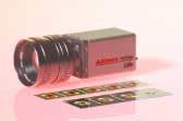
Numerous North American and European camera manufacturers are busy bringing Camera Link-based cameras to market. For example, consider the Adimec-1000m camera from Adimec Advanced Image Systems BV (Eindhoven, The Netherlands; www.adimec.com). This miniature camera measures 45 × 45 × 75 mm and uses the KAI 1020 progressive-scan, interline CCD sensor from Eastman Kodak Co. (Rochester, NY). Built as a 1000 × 1000-pixel device in a 1.1 × 1.1-in. package, this sensor offers a high level of functional integration on chip. It proves easier to interface and reduces the burden on the camera manufacturer in terms of support circuits for signal conditioning, signal processing, and other imaging functions. The chip can output 1 Mpixel of data at 30 to 48 frames/s, depending on the operating mode.
Jochem Herrmann, Adimec director of technology, says, "The Adimec-1000m camera, with a CCD sensor and digital processing, has only one-fourth of the volume of an old 1k × 1k camera. But, even using current technology, he says, "without this level of functional integration, the volume of the camera would have been, say, 10% greater."
By reducing the need for support electronics, the sensor chip also reduces cost and power. Herrmann adds, "Size is important so as not to restrict the places the camera can be used. And by using less power, it runs cooler, and that helps reliability."
The sensor's on-chip functions include a correlated double-sampling (CDS) section, electronic shutter driver, and circuits for providing various voltage levels. With on-chip voltage translation circuits, the sensor chip requires only a single 5-V supply input, although some sections of the sensor need between 8 and 12 V. The electronic shutter can translate up to 40 V. The upshot, comments Herrmann, is that the camera uses a less-expensive power supply.
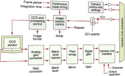
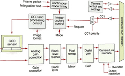
The on-chip CDS helps to maintain a high signal-to-noise ratio before signals are passed on to the camera's analog-to-digital converter. Then, the signals are presented to the camera's signal gain circuitry and, lastly, to the Camera Link interface. Herrmann comments, "If you compare the sensor with a chip that needs more voltages, external drivers, and CDS, the development time is reduced by two months, and the resulting product is more reliable because it uses fewer parts."
The sensor also provides dual outputs, with the ability to run at full 1k × 1k resolution with either one or both of the outputs operational. With progressive scan, it can run at 30 frames/s on one output or 48 frames/s with both outputs. For applications in which speed takes precedence over resolution, it can also run in interlaced mode at 49 frames/s on a single output.
Running the sensor in dual-output mode proved complicated from a systems design perspective, requiring that two image streams be integrated after digital conversion. Adimec added circuits to mirror the image data coming from one output of the sensor, which eased the camera systems integration task.
The sensor can also go to higher speeds by subsampling an image through the use of a fast line-dump feature. With this feature, unwanted rows of pixels can be clocked out quickly, which allows a small region of interest to have a higher frame rate. The sensor can also be configured with Bayer color filters as a one-chip alternative to three-chip color sensor systems.
The camera taps the highest-speed mode of the sensor and runs at 49 frames/s using both of the sensor's dual outputs and operating at 8 or 10 bits. It also supports partial scan for higher output speeds, and the desired number of vertical lines to be read out is user programmable. All camera functions, parameters, and settings are remotely controlled by software over the Camera Link interface using a basic ASCII-based protocol. This approach optimizes camera operation for a particular application. The camera uses a Windows-based control program that runs under Windows 95/98/NT/2000.
null
Incorporated into the Adimec-1000m camera, the Kodak CCD sensor includes a correlated double sampling (CDS) section, electronic shutter driver, and voltage-control circuitry. The on-chip CDS section helps to maintain a high signal-to-noise ratio before signals are passed on to the camera's analog-to-digital converter. Then, the signals are presented to the camera's signal gain circuitry and, lastly, to the Camera Link interface. All camera functions, parameters, and settings are remotely controlled by software over the Camera Link interface using a basic ASCII-based protocol.


