Imager integrates read-out IC
One of the main stumbling blocks to the rapid deployment of infrared (IR) in machine-vision systems is cost. Unlike CMOS-based cameras, it is more complex to fabricate the exotic, compound semiconductor materials used in IR focal-plane arrays (FPAs). Further, signals from each photodetector site on the FPA must be read individually using a readout integrated circuit (ROIC) that is flip-chip bonded to the sensor. This process is both time-consuming and costly, further increasing the cost of IR cameras.
If, however, it were possible to integrate the read-out electronics into the same monolithic IC—as CMOS imagers do—the cost of the devices and the cameras based around them would be greatly reduced. This concept is behind the introduction of a short-wavelength infrared (SWIR) imaging array and camera from NoblePeak Vision (Wakefield, MA, USA; www.noblepeak.com).
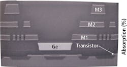
To do this, the company’s 744 × 576 TriWave (visible, near-IR, and SWIR) sensor technology integrates germanium photodetectors on a monolithic IC using a CMOS process achieving sensitivity to wavelengths from 0.4 to 1.65 μm. “The key to growing thick pure germanium with negligible defect density is dislocation trapping,” says Mike Decelle, president and CEO of NoblePeak Vision.
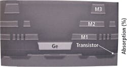
“In this process, an aperture is formed in the dielectric layer that overlies the transistors. Epitaxial growth of germanium is then used to fill the aperture and the overlying cavity.” Dislocations at the silicon-germanium interface propagate at an angle of 60° to the interface and terminate on the sidewalls of the aperture (see Fig. 1). The body of the germanium island, which is then larger than the aperture, is defect free.
After formation of the germanium sensor, alternating layers of dielectric and metal are used to interconnect readout transistors and to connect the germanium photodiode to these transistors. By allowing both reset and signal voltages to be read out at different times from each pixel, correlated double sampling (CDS) can be performed to reduce thermal noise. Designed to run at speeds up to 30 frames/s, the SWIR imager is packaged in a telecom-style butterfly package, with an integrated thermoelectric cooler (TEC) that allows the device to be cooled from 27°C to -70°C.
At the SPIE Defense & Security Symposium (Orlando, FL, USA; March 2008) NoblePeak Vision demonstrated the device in a prototype camera system. This was assembled by coupling a custom-designed sensor board and TEC controller board with a commercial three-board camera stack from Imaging Solutions Group (ISG; Fairport, NY, USA; www.isgchips.com).
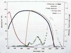
After the sensor board captures analog image data from the sensor and converts it to 12-bit image data, digital data are formatted into a standard NTSC or PAL analog video signal. This video formatting board contains a PowerPC RISC processor that reads a thermistor coupled to the imager package and adjusts the TEC accordingly. Although still in prototype stage, the company has measured the quantum efficiency of the device compared with both silicon and InGaAs devices (see Fig. 2).
The standard CMOS imager exhibits a spectral bandwidth of between 400 and 1000 nm, while the InGaAs device allows wavelengths from 900 to 1700 nm to be imaged. NoblePeak’s imager can be used to image the entire 400–1700-nm spectrum.
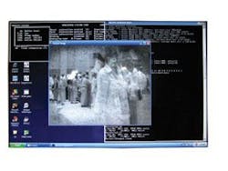
At the conference, the company also displayed uncorrected output from the camera prototype (see Fig. 3). A number of bad pixels can still be seen on the image. One of the main reasons for this, according to Decelle, was that the device used in the camera was one of the first to be fabricated. “Because the three-board camera stack from ISG contains a programmable FPGA,” he says, “bad pixel correction can easily be accomplished in hardware to produce a much more pleasing image.”
Phil Davies, vice president of sales and marketing at NoblePeak, is enthusiastic about the success of the camera. “For approximately $3000 (in 1000 quantities),” he says “we will sell OEMs the complete camera core with which to build their own cameras.” While initial applications will be in commercial and homeland security applications, the low cost of such a SWIR camera is likely to find use in many military and machine-vision applications.


