Photonics-Based Color Splitting Technique: Improving Camera Image Quality
What you will learn:
- The limitations of traditional Bayer color filters, which block significant amounts of light, limiting image quality.
- About a new photonics-based color splitting technology, which uses vertical waveguides to improve light sensitivity, resolution, and color accuracy by guiding rather than filtering light.
- How this technology could enable smaller, cheaper image sensors with more accurate color resolution.
The quest for higher quality imaging has driven continuous innovation in camera technology. However, fundamental limitations in current technologies pose challenges to further advancements. Leveraging the power and efficiency of photonics, a new solution that uses a waveguide-enabled color splitting technique can overcome the limitations of traditional color filters. New products coming to market using this approach show promise for reducing cost and size while increasing performance.
Current Limitations of Bayer Color Filters
Currently the most prevalent technology used to produce color imagery in image sensors today is the Bayer filter. This color filter array (CFA) uses a grid of red, green, and blue filters arranged in a specific pattern. While effective, Bayer filters inherently sacrifice efficiency and introduce limitations:
- Inefficiency: Color filters absorb a substantial amount of light. In fact, up to 70% of the incoming light is blocked, severely limiting the amount of light available to the sensor. This necessitates larger pixels and sensors to capture sufficient light, leading to larger, bulkier camera modules, especially in applications like smartphones.
- Resolution Limits: Bayer filters also impose a limit on image resolution. Since each pixel only captures one color component, the missing color information must be interpolated from neighboring pixels. This interpolation process can blur fine details and reduce overall sharpness.
- Color Artifacts: The interpolation process used with Bayer filters can also introduce color artifacts, such as moiré patterns and false colors, which degrade image quality.
- Scaling Challenges: As CMOS image sensor (CIS) technology advances and pixel sizes shrink, Bayer filters present scaling challenges. The need for color filters limits the ability to create sufficiently small pixels to achieve ultra-compact, high-resolution imaging.
The Smartphone Dilemma
The mobile/smartphone market represents the largest segment for CMOS image sensors, and it demonstrates the problem with current light gathering techniques.
Related: CMOS Sensors: Graphene and Quantum Dots Combine for Broadband CMOS Camera
With each successive generation of device, phone makers seek to improve the quality of the cameras in the device, largely because it has become the number one purchasing criteria consumers use to decide on a new model phone. While improvements in image quality have been steady, they come at a cost—literally, in terms of the price of the increased-sized sensors. But as importantly, this also impacts the physical size needed to house these cameras, which have knock-on effects in terms of cost, not to mention consumer’s desire for more compact phones. Challenged by the fact that the only approach to addressing the color limitations of inefficient light collection has been to increase the size of the sensors, phone makers have consistently made bigger, more expensive devices to drive camera improvements forward.
Related: Dual-Band Filters Target Price-Sensitive Applications
Vision-enabled systems in other application areas face similar challenges.
Photonics-Based Color Splitting Enables More Light to Be Captured
A new approach can solve that dilemma. It replaces traditional color filters with an advanced color-splitting technology. This approach originates from imec (Eindhoven, The Netherlands), a research and innovation hub in nanoelectronics and digital technologies. Now being commercialized by eyeo (Eindhoven, The Netherlands), the techniques used are:
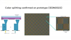
- Vertical Waveguides: The technology utilizes an array of vertical waveguides, each with a tapered section at the top that acts as an entrance funnel for incident light. These waveguides are precisely designed to guide photons and split light into colors.
- Sub-Diffraction-Limited Color Splitting: Unlike traditional color filters that absorb a significant portion of light, the solution guides all incoming light to individual pixels, maximizing light sensitivity. This architecture enables sub-0.5-micron pixels for ultra-compact, high-resolution imaging.
- CMOS Compatibility: The color splitting technology is fully CMOS-compatible and leverages silicon photonics techniques, allowing integration into existing semiconductor manufacturing processes.
Related: Novel Sensor Material Demonstrates Better Color Image Reproduction Than Silicon
Advantages of Color Splitting Technology
This technology offers a set of benefits that address the limitations of conventional color filter arrays:
- Enhanced Light Sensitivity: By eliminating absorption, it achieves a 3x increase in light sensitivity compared to traditional filters. This approach improves image quality, particularly in low-light conditions, which is critical for various applications.
- Increased Resolution: The photonics-based approach enables each pixel to capture complete color data, effectively doubling the resolution compared to Bayer filters, which inherently limit resolution due to interpolation.
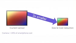
- Compact Form Factor: The increased light sensitivity allows for smaller sensors to achieve the same or better image quality. This is particularly advantageous for applications where size and weight are critical, such as smartphones, AR/VR devices, and medical imaging tools.
- Cost Efficiency: While adding waveguide structures, the technology simplifies the front-end flow by eliminating color filter deposition and micro-lens alignment, leading to a net-neutral or even favorable cost profile over time and volume production.
- Improved Color Fidelity: The technology enables native color fidelity by guiding photons directly to individual pixels, resulting in more accurate color reproduction compared to the estimation required by Bayer filters.
Target Applications
Such technology has the potential to transform a wide range of applications:
- Industrial Imaging: Industrial applications, such as machine vision and robotics, demand high accuracy, speed, and resolution. This improves inspection systems and robotic vision by delivering sharper images and higher frame rates.
- Automotive: In the automotive sector, the technology could be used to enhance the performance of ADAS (Advanced Driver-Assistance Systems) and in-cabin sensing. The increased light sensitivity and improved color capture contribute to safer and more reliable autonomous driving.
- Medical Imaging: Medical imaging benefits from compact, power-efficient, and high-fidelity imaging, enabling smaller, more portable diagnostic tools with improved image quality, leading to better patient care.
- Smartphone Cameras: In the highly competitive smartphone market, camera quality is a key differentiator. This technology enables smaller, higher-performance cameras, allowing for slimmer phone designs without compromising image quality.
- Augmented Reality/Virtual Reality (AR/VR): For AR/VR applications, compact, high-resolution, and high-sensitivity cameras are essential for creating immersive and realistic experiences. The efficiency of this approach meets these requirements, enabling advancements in AR/VR headsets and devices.
- Security and Surveillance: In security and surveillance, capturing clear images in low-light conditions is critical. High-sensitivity sensors provide a significant advantage, enhancing the effectiveness of security systems.
Related: How Machine Vision Will Help Industry 5.0 Prioritize Humans
Peer-Reviewed Paper Released
The scientific foundation of the technology was presented by researchers at the 2023 IEEE International Electron Devices Meeting (IEDM). The paper titled "Wafer-Level-Integrated Vertical-Waveguide Sub-Diffraction-Limited Color Splitters"1 details the development and demonstration of the color-splitting technology. Key highlights from the paper include:
- Demonstration of sub-micron resolution color splitting using standard backend processing on 300mm wafers.
- Tunability of color splitting via the geometry of the waveguides, enabling design to match the color sensitivity of the human eye.
- Potential for higher signal-to-noise ratio, improved color quality, and enhanced resolution for high-end cameras.
A photonics-based color splitting technology represents a leap forward in image sensing. By overcoming the fundamental limitations of traditional color filters, it enables smaller, more efficient, and higher-performance cameras across diverse applications.
References:
- S. Kang et al., "Wafer-level-integrated vertical-waveguide sub-diffraction-limited color splitters," 2023 International Electron Devices Meeting (IEDM), San Francisco, CA, USA, 2023, pp. 1-4, doi: 10.1109/IEDM45741.2023.10413746.
About the Author

Jeroen Hoet
Jeroen Hoet is co-founder and CEO of the photonics startup, eyeo (Eindhoven, The Netherlands), which develops an imaging approach to unlock maximum light sensitivity and native color fidelity for image sensors used in mobile devices, industrial systems, XR, and more. As former entrepreneur in residence at imec, a research institute, (Eindhoven, The Netherlands), he led the transition of a research-stage photonics technology into the commercial launch of eyeo in 2024.
Hoet has extensive technical and business experience in the imaging and semiconductor industries with roles in engineering, marketing, and executive management at companies such as Caeleste (Mechelen, Belgium), KLA (Milpitas, CA, USA,) and ICsense (Leuven, Belgium). He earned a master’s degree in engineering with a focus on microelectronics at Ghent University (Ghent, Belguim) and an executive MBA from Vlerick Business School (Belgium).

