Image processing speeds wafer analysis
By Andrew Wilson,Editor
Integrated circuits are manufactured by depositing materials composed typically of silicon or gallium arsenide in layers on a wafer substrate. The physical characteristics of the substrate of each thin-film layer are critical in the successful implementation of chip design. However, production time of hours or even days can be lost if an integrated circuit is implemented on a faulty substrate or thin-film layer. To verify the integrity of the substrate and how precisely subsequent layers of material are deposited on it, a process known as reflection high-energy electron diffraction (RHEED) is commonly used.
In the RHEED process, a high-energy electron beam ranging from 10 to 50 keV is directed at an angle to the wafer surface. Electrons are diffracted by the crystal structure of the wafer and then impinge on a phosphor screen mounted opposite to the electron gun. The resulting effect is a series of streaks, with the distance between the streaks indicating the surface lattice unit cell size on the wafer. If a surface is atomically flat, then sharp RHEED patterns are seen. However, if the surface is coarse, the RHEED pattern becomes diffuse and spotty.
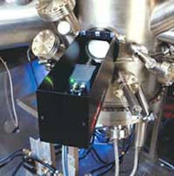
By capturing and analyzing an image of the wafer or chip surface, engineers can discern the structural integrity, thickness, and rate of deposition on the chip after manufacture. Systems-integrator k-Space Associates (kSA; Ann Arbor, MI) has improved this electron diffraction technique with the introduction of the kSA-400 PC-based system that enables engineers to measure wafer film growth in real time (see Fig. 1). During operation, this system quantifies surface perfection, thickness, growth rate, and atomic spacing.
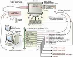
SYSTEM DESIGNAllowing engineers to analyze static diffraction patterns and acquire data during high-speed substrate rotation, the kSA-400 system has been developed for both static and real-time image acquisition and analysis. Determination of lattice spacing, strain evolution, growth rate, thickness, coherence lengths, and reconstruction evolution are all controlled using the system's graphical user interface. After images are captured, they can beanalyzed using these standard functions or, alternatively, they can be analyzed by custom analysis routines.During kSA-400 operation, a RHEED electron gun directs a beam across a chamber containing the semiconductor wafer. Within the chamber, a number of source cells containing the material to be deposited are held in crucibles. As these crucibles are heated, the material within them evaporates. By controlling shutters placed over the crucibles, the wafer's thin-film deposition rate and thickness can be controlled. The resultant images are then analyzed using an imaging system integrated within the kSA-400 system.
To detect the series of streaks that impinge on the phosphor screen, a KPM2 CCD camera from Hitachi Denshi America (Woodbury, NY) with 768 x 480 x 8-bit resolution is used. Darryl Barlett, kSA general manager, says, "Unfortunately, in some cases the diffraction pattern is weak, and extended integration periods must be used to overcome thermal noise." Accordingly, Barlett and his colleagues modified the design of the camera with a Peltier cooler to reduce the effects of thermal noise and to increase the signal-to-noise ratio (see Fig. 2).
After images are captured by the camera, they are delivered in RS-170 format to a DT3152 PCI-based frame grabber from Data Translation (Marlboro, MA). "One of the distinguishing features of the DT3152," says Barlett, "is that it has programmable resolution, so the full 768-pixels/line horizontal resolution of the camera is captured in a one-to-one mapping from camera to frame grabber." Custom software developed using Data Translation DT Open Layers software-development kit (SDK) is used to digitize images in the host computer. The frame-grabber SDK allowed kSA to meet the customers' special requirements by using different Data Translation frame grabbers as needed without rewriting existing code. According to Barlett, these included the DT3153 and DT3154 frame grabbers for customers who needed to capture color diffraction images.
After images are captured in host memory, they must be analyzed, enhanced, and displayed. "To do so," says Barlett, " we looked at a number of off-the-shelf image-processing packages including the Intel Corp. (Santa Clara, CA) image-processing library." Unfortunately, no commercially available software packages could support varying bit-depth images (up to 96 bits) resulting from image summation. Therefore, images captured using the DT Open Layers SDK were imported into Microsoft Visual C++ environment. All the image-processing functions, such as image filtering, background subtraction, analysis, and display, were developed in this environment.
CONTROL AND INTEGRATIONWhile developing the image-processing functions, engineers discovered that the kSA-400 design presented a problem in that the entire system also needed to be controlled using the same operator interface. To solve this problem, kSA engineers developed and purchased a number of PCI boards to control the RHEED electron gun and shutter-control unit."To control the deposition process accurately," says Barlett, "system demands mandated that the kilovolt-power supply is accurately controlled." But because power supplies for such guns cannot be readily purchased, kSA engineers developed a custom unit for the purpose. To accurately control this power supply, an eight-channel, 16-bit DT334 digital-to-analog (D/A) converter board from Data Translation was integrated into the PCI card cage of the host computer. This data-acquisition card is controlled from the operator interface, also developed using Microsoft Visual C++.
The kSA engineers purchased another off-the-shelf board to control the shutter-deposition unit. This time, Barlett integrated a KPCI-PIO24 PCI-bus 24-channel, parallel, digital I/O board from Keithley Metrabyte (Cleveland, OH) to control the status of switches that direct operation of the eight-shutter control unit.
As the wafer is cut along a certain plane, the atoms near the surface could be disturbed and could lead to changes in the relative positions of the surface atoms. Such changes can be explored with a low-energy electron diffraction process by bombarding the surface with electrons of approximately 1-1000 eV. Diffracted electrons then appear as spots on the phosphor screen.
"Such systems demand different power controllers than those used in RHEED systems and therefore require different power supplies and controllers," says Barlett. To accommodate these power supplies, the kSA-400 system also uses a DAC-02 board from Measurement Computing (Middleboro, MA). This low-cost 12-bit D/A converter board controls a proprietary power-supply controller.
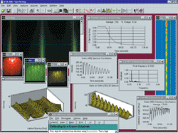
For real-time acquisition and analysis, the system's scan mode allows the technician to extract data from the evolving RHEED pattern. In this way, pertinent diffraction data can be extracted under reduced data-storage requirements (see Fig. 3). Linescan data are stacked in time, forming scan-mode images that show the evolution of the diffraction pattern. In addition, screen windows can be stored in their entirety. They form area images similar to scan-mode images. When analyzed on-the-fly, only the resultant window analysis data are stored, such as peak intensity, average intensity, and centroid positions.
Acquired image data also can be stored and played back as video movies, with full analysis capability. A live video window shows the windows and lines that can be extracted during the run. By setting the tracking to peak, each window locks on to and centers on its peak intensity during a run. Real-time window analysis shows the evolution of the peak intensity within each window during a scan-mode run. A real-time line profile shows the profiles of the diffraction lines. In this way, the technician can monitor the evolution of diffraction peaks and noise.
Recent improvements in electron-gun brightness allow diffraction-pattern acquisition to be done at faster rates. To provide their customers with faster speed, kSA has introduced an optional 110-frame/s rate to the kSA-400 system. Having a 1/3-in. progressive-scan, interline-transfer CCD camera from Uniq Vision (San Clara, CA), the system features 10-bit, 659 x 494-pixel resolution. According to Barlett, this faster rate allows more accurate-growth determination and faster monitoring of time-event features such as lattice spacing, strain, and reconstruction. Barlett says, "To meet the faster speed demands, the Uniq camera was interfaced to the PXD 1000, EIA-644 (LVDS), 40-MHz-per-channel frame grabber from CyberOptics (Portland, OR)."
Company InformationCyberOpticsPortland, OR 97223Web: www.imagenation.comData Translation
Marlboro, MA 01752
Web: www.datx.com
Hitachi Denshi America
Woodbury, NY 11797
Web: www.hdal.com
Keithley Metrabyte
Cleveland, OH 44139
Web: www.keithley.com
k-Space Associates
Ann Arbor, MI 48103
Web: www.k-Space.com
Measurement Computing
Middleboro, MA 02346
Web: www.measurementcomputing.com
Uniq Vision
San Jose, CA 95133
Web: www.uniqvision.com


