Near infrared imaging: Process improvements boost NIR quantum efficiency
Capturing images at very low light levels is critical for many medical, scientific, military and security imaging applications. Doing so requires image sensors that exhibit a high quantum efficiency (QE), a low read out noise and dark current, as well as a wide dynamic range that allows high spatial resolution imaging across a range of illumination conditions.
Recent developments in CMOS imagers have led to an expanding array of low-light-level cameras. Many of which, are finding use in night-vision applications that require color image sensors during the day and near infrared (NIR) illumination at night.
Because there are more NIR photons than visible photons at night, NIR technology enables higher-resolution image capture with fewer power-hungry LEDs, extending the life of battery-powered security camera applications.
Having said that, since the wavelength of NIR illumination is outside of the visible spectrum, developers of machine vison and imaging systems also rely on NIR lights in applications where avoiding interference with the surrounding environment or minimizing human visual distraction are important.
Other growing application areas include automotive driver-side monitoring applications for detection of drowsy or distracted drivers, as well as biometric applications such as facial and iris recognition systems.
However, as useful as these capabilities might be, existing approaches to NIR detection lack the NIR sensitivity required for many emerging next-generation mobile, embedded, AR/VR and security camera imaging applications.
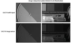
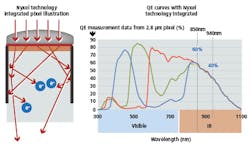
Tested under 850 nm IR LED illumination, the OV2770 sensor with Nyxel technology is significantly brighter, with improved signal to noise ratio and no reduction in image sharpness.
Understanding this, OmniVision Technologies, Inc. (Santa Clara, CA, USA;www.ovt.com) has developed a new approach to NIR imaging dubbed Nyxel technology, which leverages novel silicon semiconductor architectures and processes.
Nyxel combines thick-silicon pixel architectures with careful management of wafer surface texture to improve QE, along with extended deep trench isolation (DTI) to help retain (modular transfer function) MTF without affecting the sensor's dark current.
Increase QE 3 to 5x
After applying the technology as a test case to an OmniVision OV2770 2.8 μm back-side illuminated CMOS image sensor, results show a QE increase of up to 3x at 850 nm and 5x at 940 nm, when compared to the same sensor without Nyxel. One significant change was doubling the epitaxial layer thickness from about 3 to 6 microns, according to Boyd Fowler, OmniVision's Chief Technology Officer.
"QE is the probability of collecting an electron given a photon enters the substrate," Fowler explains. "It's a function of photon path length, so the thicker the silicon the better the absorption."
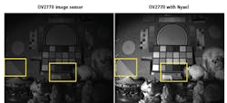
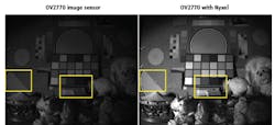
Zoomed in on the yellow rectangles in the figure above shows that Nyxel technology (top) provides greater sensitivity with little-to-no reduction in spatial resolution.
One drawback to this approach, however, is that when electrons are absorbed very deep, they tend to diffuse to their local neighbors, which can cause problems like a reduction in spatial resolution. To address this issue, Nyxel technology includes extended DTI around each pixel using silicon dioxide.
"When the electrons are generated in the substrate, they need to be collected. This DTI makes sure these electrons can't easily move from the pixel where they are generated to an adjacent pixel, which is critical for effective isolation and enables higher sensitivity, without compromising spatial resolution," Fowler notes.
Wafer surface texture is key
Perhaps most important to the new process is careful management of wafer surface texture to scatter the light as it enters the pixel. By scattering the light, the photons must travel a significantly longer path length.
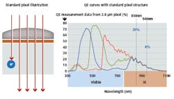
A standard CMOS image sensor pixel illustration and its QE curve (a), where its structure causes the normally incident light to move straight through the silicon. The same sensor enhanced with Nyxel technology (b) and its QE curve, where the special silicon surface treatment causes similar light to bounce around, increasing the chances of photo-electron conversion.
"In this case, the straight path length has been extended from about 3 or 4 microns maximum in our legacy design, to a scattered path of up to 10 or 20 microns with the Nyxel technology," notes Fowler. "As light enters, it bends and scatters at the surface, and because the index of refraction of the silicon dioxide in the DTI is much lower than the index of refraction of the silicon, it acts like a fiber optic, with light bouncing off the silicon dioxide, yet remaining inside the pixel, which not only allows for the longer path length, but also makes sure the photons are confined to the pixel where they should be."
OmniVision is currently sampling this experimental 2MP Nyxel technology-based product to demonstrate the proof of concept, and has also launched a 5MP product in the security market in October of this year. For 2018, the company has a slew of various resolution Nyxel-based products on the roadmap for the security market throughout Q1 and Q2, and very quickly after that will be looking at products for the machine vision market, AR/VR, automotive and medical applications.
In battery-powered security applications that require color image sensors during the day and near infrared (NIR) illumination at night, this higher sensitivity Nyxel technology should enable OmniVision customers with the ability to reduce the total illumination power and extend battery life. For powered security applications, with the same LEDs, customers should be able to extend sensor range to see farther into the night.
For future products in other markets, Nyxel technology should enable machine vision and imaging system developers to work under lower light conditions, achieve power savings, and in some cases reduce the size and cost of their designs by minimizing the number of LEDs, power drivers, and heat sinks.
"In the past people have tried to develop better NIR technology, but it was almost always a tradeoff between higher sensitivity and spatial resolution," says Fowler. "This technology enables us to give the customer both at the same time."