Early applications for hybrid CCD in CMOS sensor cameras include digitizing film, as well as electronics and semiconductor inspection.
High quality illumination is one key to success for machine vision system designers, especially in high speed, high resolution line-scan applications. After all, the greater the line speed, the greater the demand for light due to reduced time available for charge accumulation in each pixel.
Time Delay Integration (TDI) is essentially a line scan imaging method that increases sensitivity by oversampling the scene across a plurality of line sensors, which are synchronized in a time-delayed fashion with the relative motion between the scene and line sensors. By adding the charges from multiple line sensors, the signal-to-noise ratio is increased, producing images with sufficient contrast, even at higher speeds.
Until recently, TDI cameras have relied exclusively on CCD technology due to the ease with which charges are transferred from one CCD gate to the next. Since the signal remains in the charge domain, as the charges transfer and accumulate from one line to the next, there is typically little to no noise contribution involved.
Charge vs voltage domain
CMOS technology, however, is different in that it converts signals at the pixel level, transforming from the charge domain to the voltage domain, which tends to add noise to the process. While there have been some attempts in applying CMOS technology to TDI sensors, explains Wojciech Majewski, International Sales Director, Vieworks (Gyeonggi-do, Republic of Korea; www.vieworks.com), they haven’t become commercially successful.
“That is, until early 2016, after several years of stealth sensor development, when Vieworks introduced the first commercial TDI cameras based on proprietary hybrid sensors combining CCD and CMOS imaging technologies,” Majewski explains. “The underlying CMOS structure of the sensor with built-in A/D converters permits high-readout speed and digital output, increasing the line speed by a factor of four.”
“At the same time, there is no need to add expensive and complex external support circuitry to convert the analog data from the sensor to digital pixels. This helps reduce heat generation which would have been generated by the extra electronics typically required by CCD technology and keeps the camera cool, minimizing the noise generated by excessive heat,” says Majewski, adding that “the CMOS sensor also greatly diminishes power consumption.”
“The breakthrough of this TDI sensor design was incorporating the CCD photosites on top of the CMOS sensor and by using a CCD pixel array, the image quality is improved in terms of signal-to-noise ratio,” Majewski explains, adding that “the integration process in CCD technology does not add any noise because it involves the charge transfer, so you get the high TDI sensitivity benefits of CCD gates and high speed and system integration benefits of CMOS.”
Early applications abound
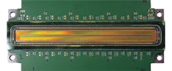
In two years since its formal introduction, Vieworks has brought more than 20 different hybrid TDI camera models to market, ranging from 3k x 32 to 23k x 256 (Figure 1). In addition to monochrome, color models are also available.
Figure 1: The Vieworks 23k x 256 Hybrid TDI sensor combines the high TDI sensitivity of CCD gates with the high speed and system integration benefits of CMOS technology.
“Over a hundred different customers requiring high-speed and light-sensitive applications have adopted these cameras, and thousands have been delivered and integrated into machine vision systems,” notes Majewski.
The majority of applications are in traditional electronics and semiconductor automated optical inspection such as flat panel display (FPD) and FPD component inspection, as well as wafer inspection and printed circuit board inspection.
“These hybrid TDI cameras have been quickly adopted, as manufacturers and their equipment suppliers have started phasing out the traditional TDI technologies, and others have started replacing traditional line-scan cameras to gain improvements in light sensitivity and line speed for a modest cost increase,” says Majewski.
Chip-on-film inspection
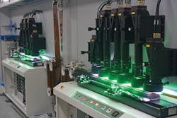
One such application is chip-on-film (COF) inspection. WarpVision (Suwon, Republic of Korea www.warpvision.co.kr) has developed a COF inspection system that uses a Euresys (Angleur, Belgium; www.euresys.com) Coaxlink Quad frame grabber and Open eVision libraries to capture images from six Vieworks VT-18K cameras (Figure 2).
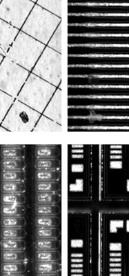
Figure 2: WarpVision Chip-On-Film inspection systems uses a Euresys Coaxlink Quad frame grabber and Open eVision libraries to capture images from six Vieworks VT-18K cameras. Inset images show defects taken with a TDI camera at 1 µm resolution. Courtesy of WarpVision Inc.
The system inspects the circuits as well as the surface of the film, checking for defects such as scratches, stains, foreign particles, film residue, contamination, corrosion, discoloration, position, color, character, and missing or unwanted extra patterns.
“We previously developed large-capacity high-speed processing technology including an image-processing library optimized for line-scan cameras,” explains WarpVision R&D manager Mr. Kim. “But with the miniaturization of COF products and resulting increase of image data, we needed a faster, more accurate, and higher-resolution TDI camera. The Vieworks 18K TDI camera was the largest resolution available on the market and it met our requirements perfectly. The end result was an ultra-fast, large-area inspection technology.”
Secure data preservation
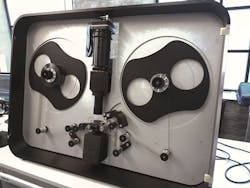
PIQL AS (Drammen, Norway; www.piql.com), known for digitizing film, has adapted their technology for secure, offline, data preservation out of reach of cyber-attacks. The company’s PiqlReader system, shown in Figure 3, scans, digitizes and converts data to film, which is then stored in its disaster-proof vault called the Arctic World Archive, that can reportedly preserve the data for over 500 years.
Figure 3: PIQL AS uses an Active Silicon FireBird CoaXpress frame grabber paired with highly sensitive Vieworks VT12K-5KX TDI camera in its PiqlReader system to efficiently read back encrypted data from film, ensuring error-proof information extraction.
PIQL engineers specified a Vieworks VT12K-5KX TDI camera due to its sensitivity, low price and dimensions that allowed retrofitting existing scanners without mechanical rework. The camera connects to the system using a FireBird CoaXpress frame grabber from Active Silicon (Iver, UK; www.activesilicon.com) to capture the images with the encrypted data.
“From a new product development prospective, the sensitivity was the most appealing factor,” explains PIQL R&D manager Alexey Matantsev.
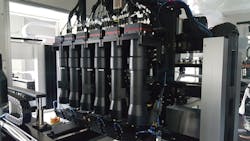
Another application is Sungwoo Techron (Changwon city, Republic of Korea; http://www.swmv.co.kr). The company uses Vieworks VT-12K cameras in its Auto Vision Inspection Machine (AVIM) inspection equipment that is designed for inspection of all types of lead frames and pre-molded LEDs (Figure 4).
Figure 4: Sungwoo Techron uses six VT-12k TDI cameras in its Auto Vision Inspection Machine that is designed for inspection of all types of lead frames and pre-molded LEDs.
“We needed a low-power, low-noise, line-scan camera with high signal-to-noise ratio at a reasonable price,” explains Mr. Park, Sungwoo Techron product manager. “We tested Vieworks TDI cameras extensively and found out that instead of settling on line scan, we could actually use TDI cameras with superior results for a fraction of the incremental cost.”
Single image processed by two frame grabbers
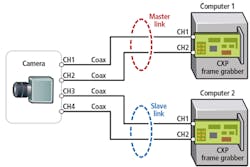
Another reason Sungwoo chose to adopt VT-12K from Vieworks is the ability to use a Multi-Link function. In a CoaXPress Multi-Link configuration, the camera enables the transmission of the data stream from a single camera to multiple frame grabbers, which could be installed in separate computers.
In this application, Sungwoo Techron engineers specified two Radient eV-CXP frame grabbers from Matrox Imaging (Dorval, QC, Canada; www.matrox.com/imaging) to communicate with each camera. As shown in Figure 5, the camera transmits image data via two channels to one frame grabber and the remaining channels transmit to the other.
Figure 5: Multi-Link Configuration of the VT-12 camera and two Matrox frame grabbers.
Sunwoo used CH1 and CH2 channels to serve as a ‘Master Link’ and the CH3 and CH4 channels as a ‘Slave Link’. Parallel processing on two different workstations effectively doubled the image processing speed.
In the AVIM machine, Sungwoo Techron implemented their unique multi-scan method to detect incorrect lead spaces, misalignments, plating shifts, scratches, oxidation, stains and other defects. Besides inspecting plating and non-plating areas, the system is also capable of inspecting and finding manufacturing defects in pit/pin holes and lead frame heads.
Other applications for such hybrid TDI cameras include remote sensing in in UAVs as well as large and small satellites, and life science applications including DNA sequencing, cell cytometry and pathology.
Companies mentioned:
Active Silicon
Iver, UK
www.activesilicon.com
Euresys
Angleur, Belgium
Matrox Imaging
Dorval, QC, Canada
PIQL AS
Drammen, Norway
Sungwoo Techron
Changwon city,
Republic of Korea
Vieworks
Gyeonggi-do,
Republic of Korea
WarpVision
Suwon, Republic of Korea
About the Author

John Lewis
John Lewis is a former editor in chief at Vision Systems Design. He has technical, industry, and journalistic qualifications, with more than 13 years of progressive content development experience working at Cognex Corporation. Prior to Cognex, where his articles on machine vision were published in dozens of trade journals, Lewis was a technical editor for Design News, the world's leading engineering magazine, covering automation, machine vision, and other engineering topics since 1996. He currently is an account executive at Tech B2B Marketing (Jacksonville, FL, USA).
B.Sc., University of Massachusetts, Lowell

