Advancing Precision in Semiconductor Manufacturing
Wafer bumping is an essential process in modern semiconductor manufacturing that establishes electrical and physical connections between integrated circuits (ICs) and their external environment. As the complexity and interconnect density of chips continues to rise, ensuring the quality of microscopic bumps on wafers is becoming increasingly important. Machine vision engineers and integrators may face challenges in acquiring precise 3D measurements from highly reflected, tiny surfaces with stringent process tolerances.
Here, we look at the technical aspects of a next-gen 3D camera system designed specifically for wafer bump inspection, focusing on how advanced optical principles, sensor technologies, and FPGA-based processing work together to meet demanding inspection requirements.
Wafer Bumping and Its Challenges
Wafers form the physical substrate for billions of semiconductor devices powering the digital age. Bumping involves fabricating microscopic metal protrusions (bumps) on the wafer surface to enable chip-to-package or chip-to-chip electrical connections. These bumps typically undergo photolithography, plating, and reflow processes to achieve diameters as small as 10 microns in advanced applications.
High-performance computing (HPC) processors such as CPUs, GPUs, and AI chips rely on densely packed, area array bump layouts to improve interconnect density and reduce electrical path lengths. These advancements demand rigorous quality control in bump height, diameter, pitch accuracy, and coplanarity to ensure signal integrity and overall device reliability.
With bump dimensions in the micron range and metallic surfaces exhibiting strong reflectivity, traditional optical inspection methods might struggle with specular reflections and glare that obscure fine surface details; halation interference caused by complex lighting reflections; shadowing effects that hinder consistent visualization across spherical bump geometries; and measurement inaccuracies due to parallax, magnification variation, and lens distortion.
Inspection systems must overcome these optical hurdles while delivering submicron measurement precision and high throughput to align with semiconductor manufacturing cycle times.
3D Structured Light Camera
Taking a 12’-in. wafer as an example, thousands of bumps must be inspected, and each is 70 μm in height with a 75 μm dia., and with a 150 μm pitch. To ensure optimal electrical connection, the automated optical inspection vision solution is expected to meet the following stringent process tolerances:
· Height tolerance (relative to reference plane): ≤ ±3 um
· Diameter tolerance ≤ ±2 um
· Pitch tolerance (true position) ≤ 3 um
· Global coplanarity tolerance ≤ 3 um
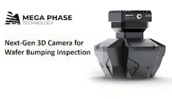
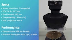
A possible solution for these challenges could be a 3D structured light camera specifically designed for bump inspection. The resolution and field of view for a device from Mega Phase Technology (Shanghai, China) is a 21-megapixel area scan sensor that can capture a 14.6 x 11.7 mm field of view covering tens of thousands of bumps with more than 200 pixels for both. The camera offers XY spatial interval of 2.85 µm; XY repeatability less than or greater than 0.2 µm; Z repeatability ≤ 0.05 µm.
It also offers temporal noise under 3.5 electrons rms, full-well capacity ≥ 32,000 electrons, and a dynamic range exceeding 68 dB to ensure stable imaging despite the reflective bump surfaces.
The system uses a doubly telecentric lens to reduce optical distortions, aiming to achieve accurate height and diameter measurements for bump validation.
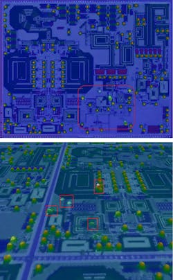
To combat the challenges of glare and shadow, the camera incorporates four integrated projectors that sequentially cast fringe patterns for multiple orientations. This multi-orientation projection aims to mitigate specular reflection interference, compensate for shadowing effects on spherical bump surfaces, and suppress stray light to preserve measurement fidelity. The resulting point cloud data is made to be comprehensive, stable, and shadow-free, providing a basis for metrology and bump inspection.
FPGA-Based On-board Processing for Throughput
High-volume semiconductor manufacturing requires not only precision but also speed. Traditional approaches that transmit raw images to external processors could induce latency and bottlenecks. This camera system is designed to integrate FPGA-based on-board computing that can acquire and process 3D structured light data within 200 ms per exposure and perform 3D reconstruction onboard in less than 500 ms, outputting processed point cloud data.
This hardware-accelerated pipeline supports parallelization of image capture, data computation, and stage motion, enabling an inspection cycle time sufficient to handle 5 to 10 wafers per hour for 12-inch wafers.
Pixel-Level Alignment of 2D and 3D Data
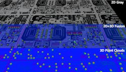
Inspection demands include both geometric measurements (3D height, coplanarity) and surface defect detection (2D diameter, pitch, and defect analysis). This system is designed to produce high-resolution 2D grayscale images and 3D point clouds aligned at the pixel level in a single snapshot. Benefits of this alignment can include streamlined inspection workflows by integrating 2D and 3D data, accurate cross-referencing of bump positional and surface defect attributes, and simplified verification logic, which can lead to faster defect detection and yelled analysis.
The system aims to perform 2D metrology within the duration of the 3D measurement, enabling throughputs of up to 14 wafers per hour without compromising accuracy.
Author bio: Zhenying Hu is overseas marketing specialist at Mega Phase Technology (Shanghai, China). She has been dedicated to providing global partners and customers with actionable insights and a deep understanding of advanced 2.5D and 3D vision.


