Powering Embedded Vision with Image Sensors
Marie-Charlotte Leclerc, Product Manager, Teledyne e2v ( Grenoble, France; https://imaging.teledyne-e2v.com/).
New imaging applications are booming, from collaborative robots in Industry 4.0, to drones fighting fires or being used in agriculture, to biometric face recognition and point-of-care handheld medical devices at home. A key enabler in the emergence of these new applications is more accessibility for embedded vision. Embedded vision is not a new concept—it simply defines systems that include a vision setup that controls and processes data without an external computer. It has been widely used in industrial quality control in the form of what are generally referred to as “smart cameras”.
A recent change is the availability of affordable hardware components developed for the consumer market, which has drastically reduced the bill-of-material and their size compared with computers. For example, small integrators/OEMs can find single-board computers or system-on-modules, such as the NVIDIA Jetson, in low volume, whereas larger OEMS can directly supply image signal processors, such as Qualcomm’s Snapdragon. At the software level, off-the-shelf libraries have made specific vision systems much faster to develop and easier to deploy, even in fairly low quantities.
The second change that is fueling the growth of embedded vision systems is the emergence of machine learning, which enables neural networks in the lab to be trained and then uploaded directly into the processor so that it can autonomously identify features and make decisions in real-time.
Providing solutions adapted to embedded vision is critically important to companies in the imaging industry that wish to target these high-growth applications. Image sensors, which directly affect the performance and design of embedded vision systems, play a major role for larger adoption and its key drivers can be summarized by the SWaP-C acronym: decreasing Size, Weight, Power and Cost. A strong accelerator for new uses of embedded vision is to meet market acceptable price points, which comes with a strong constraint on the vision system cost.
Optics Cost Savings
The first way to cut vision system costs is to reduce its footprint for two reasons:
- As the image sensor pixel size decreases, the intrinsic silicon cost shrinks because more chips can fit on the same wafer.
- The sensor can fit in smaller and lower cost optics.
For image sensor manufacturers, this reduced optical cost has another impact on the design. As a general rule, the lower the optics cost, the less optimal the angle of incidence on the sensor is. Therefore, low-cost optics require the design of specific shifted microlenses positioned on top of the pixels so that they compensate for the distortions and focus light coming from wide angles.
Cost-Effective Interfaces
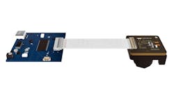
Aside from optical optimization, the choice of interface also indirectly impacts vision systems costs. The MIPI CSI-2 interface is the most suitable candidate to enable interface-induced cost savings as it was originally developed for the mobile industry by the MIPI Alliance. It has been broadly adopted by most ISPs and has begun to be adopted in industrial markets as it offers a lean integration in the cost-effective system-on-chip (SoC) or system-on-module (SoM) from NXP, NVIDIA, Qualcomm, Rockchip, Intel, and others. Designing a CMOS image sensor or imaging module with a MIPI CSI-2 interface provides a direct data transfer from the image sensor to the host SoC or SoM of the embedded system without any intermediate converter bridge, which saves cost and PCB surface, and, of course, that advantage is even stronger in embedded systems based on multiple sensors for 360° vision.
These benefits come with some constraints. The MIPI CSI-2 D-PHY standard, today widely used in the machine vision industry, relies on highly cost-effective flat cables with the drawback of a connection distance limited to 20 cm, which may not be optimal in remote head setups where the sensor is located farther from the host processor. This is often the case in traffic monitoring or surround-view applications. One solution for longer connection distance consists of placing additional repeater boards between the MIPI sensor board and the host processor—at the expense of miniaturization. Other solutions exist, coming not from the mobile industry but from the automotive industry this time: the so-called FPD-Link III and MIPI CSI-2 A-PHY standards supporting coax or differential pair cables allow connection distances up to 15m.
Reducing Development Costs
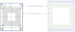
Rising development costs often present a challenge when investing in a new product. It can cost millions of dollars in non-recurring expenses (NRE) and create pressure on the time to market. For embedded vision, this pressure becomes even stronger as modularity (which is defined by the ability to switch image sensors), is an important value for integrators. Fortunately, the NRE can be limited by offering certain degrees of cross-compatibility between sensors, for example, by defining families of components sharing the same pixel architecture to have steady electro-optical performances, by having common optical centers to share a single front mechanics, and a compatible PCB assembly, by means of footprint or pin-to-pin compatibility, to fasten evaluation, integration, and supply chain as illustrated in Figure 1.
Nowadays, developing embedded vision systems has become even faster and more affordable with the broad release of so-called modules and board-level solutions. These turnkey products usually consist of a ready-to-integrate sensor board that sometimes also includes a preprocessing chip, a mechanical front face, and/or a lens mount. These solutions benefit applications through their highly optimized footprint and standardized connectors, which enable direct connection to off-the-shelf processing boards such as NVIDIA Jetson or NXP i.MX units without the need to design or manufacture intermediate adapter boards. These modules or board-level solutions not only ease and fasten hardware developments by removing the need for PCB design and manufacturing, but also drastically shorten software developments, as they are provided along with their Video4Linux drivers most of the time. OEMS and vision system makers can therefore skip weeks of development in making the image sensor communicate with the host processor to instead focus on their differentiating software and overall system design. Optical Modules can push that turnkey aspect one step further by also integrating the lenses inside the modules, providing a full package from the optics to the driver through to the sensor board and eliminating tasks related to lens assembly, and testing.
Energy Efficiency for Enhanced Autonomy
Miniature battery-powered devices are the most obvious applications benefiting from embedded vision, as external computers prevent any portable applications. To decrease the systems’ energy consumption , image sensors now include a multitude of features that enable the system designers to save power.
From the sensor standpoint there are multiple ways to decrease power consumption in an embedded vision system without decreasing the acquisition frame rate. The simplest way is at system level by minimizing the dynamic operation of the sensor by using (as much as possible) the sensors’ standby and idle modes to reduce the power consumption of the sensor itself. Standby mode enables the sensor’s power consumption to be reduced to a small percentage of the functional mode by switching off the analog circuit of the sensor. The idle mode saves around half of the power consumption and can prepare the sensor to acquire images in microseconds.
Another way to save power is to design a sensor using more advanced lithography nodes. The smaller the technology node, the lower the voltage necessary to switch the transistors and lowering the dynamic power consumption as it is proportional to voltage square: P_dynamic∝C×V² . Therefore, pixels that were using 180-nm technology 10 years ago have shrunk by reducing the transistors to 110 nm and also decreased the voltages of the digital circuit from 1.8 to 1.2 V. In the next generation of sensors, the 65-nm technology node will be used to provide even more power savings for embedded vision applications.
Lastly, an image sensor can be appropriately chosen to reduce the energy consumption of the LEDs in certain conditions. Some embedded systems rely on active illumination, for example, to generate a 3D map, to freeze motion, or to simply increase the contrast by using sequentially pulsing specific wavelengths. In these cases, the image sensor can generate power savings by lowering the noise of the sensor when operating in light-starved situations. By lowering the sensor noise, engineers can decide either to reduce the current intensity or the number of LEDs integrated in the embedded vision system. In other conditions, where image capture and LED flash are triggered by an external event, choosing the appropriate sensor readout architecture can lead to significant power savings. Whereas conventional rolling shutter sensors require LEDs to be turned ON during the whole exposure of the frame, global shutter sensors allow it to turn ON the light for only a portion of frames. Switching from rolling to global shutter image sensors, therefore, induce lighting costs savings while still maintaining the noise as low as the CCD sensors used in microscopy if using in-pixel correlated double sampling.
On-Chip Functionalities Pave the Way for Application-Designed Vision Systems
An extreme extension of this embedded vision concept would lead us to a full customization of the image sensor integrating all the processing functions (SoC) in a 3D stacked fashion to optimize performance and power consumption. However, the cost of developing such a product would be tremendously high. While it is a custom sensor, it is not totally impossible to reach that level of integration in the long term. Today we are at an intermediary step, consisting of embedding specific functions directly into the sensor to reduce computational load and speed processing time.
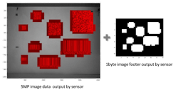
For example, in barcode reading applications, Teledyne e2v has patented an embedded feature directly on the sensor chip that contains a specific barcode identification algorithm to locate the position of the barcodes in each frame, so the ISP can focus on the these regions to process data more efficiently.
These functionalities are often specific and require a good understanding of customers’ application. As long as the application is sufficiently understood, other on-chip functionalities can be designed to optimize the embedded vision system.
Reducing the Weight and Footprint to Fit in the Smallest Spaces
A major requirement for embedded vision systems is to fit in small spaces or to be lightweight to fit within handheld devices and/or maximize battery-powered engines. That’s why today, most embedded vision systems use small optical format sensors with a limited resolution from 1 to 5 MPixels.
Reducing the dimensions of the pixel array is only the first way to reduce the footprint and weight of the image sensor. Today, the 65-nm process enables us to decrease the global shutter pixel pitch down to 2.5 µm without damaging electro-optical performances. Such manufacturing processes lead to products such as a full HD global shutter CMOS image sensor in the same format as in the mobile phone market, i.e. less than 1/3 in.
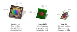
Another key technology for reducing sensor weight and footprint is to reduce dimensions of the package. Wafer-level packages have experienced fast growth on the market for a few years, especially for mobile, automotive, and medical applications. Compared with the classical Ceramic Land Grid Array (CLGA) packages used in the industrial market, the wafer-level fan-out packages and chip scale packages provide higher density connections, an excellent solution to the challenge of producing miniature and lightweight image sensors for embedded systems. In the case of Teledyne e2v’s 2-Megapixel sensors, the combination of wafer-level packaging with smaller pixel sizes allows to divide by four over five years only.
Looking to the future, we can expect another technology to bring further reductions in the size of sensors for embedded vision.
3D stacking is an innovative technique to make semiconductor components by manufacturing the different circuit blocks on separate wafers, and then stacking and interconnecting them with Cu-Cu connections and Through Silicon Vias (TSV). 3D stacking allows devices to be made with smaller footprints than conventional sensors because of layer overlap. In 3D stacked image sensors, the readout and processing blocks can be moved below the pixel array and row decoder. The footprint therefore decreases by the surface of the readout and processing blocks, while also bringing the possibility to add extra processing power in the sensor to unload the image signal processor.

However, 3D stacking currently faces some challenges in order to be widely adopted on the image sensor market. First this is an emerging technology, secondly it’s higher cost because of the additional process steps required that increase the silicon cost by more than three times compared with conventional technology wafers. Therefore, 3D stacking will be an option mostly for high-performance or very small footprint embedded vision systems.
Embedded vision can be summarized as doing “lean” vision and can be applied by a number of companies including OEMs, system integrators, and standard camera manufacturers. “Embedded” is a generic term that is used in many applications, which makes it difficult to set a single list of specifications. However, several rules apply to optimize embedded vision systems, as the driving markets are generally not driven by state-of-the-art speed or sensitivity but rather by size, weight, power, and cost. The image sensor is a significant contributor to these parameters, and care is needed in the choice of the image sensor that will optimize overall embedded vision system performance. The right image sensors will offer more freedom for an embedded vision designer to reduce not only the bill of material but also the footprint of both illumination and optics. But even more than image sensors, the emergence of turnkey board-level solutions under the form of imaging modules paves the way toward further optimization of size, weight, power, and cost and a significant decrease of development cost and time, delivering affordable and deep learning-optimized image signal processors from the consumer market, without adding complexity.