PHOTOVOLTAICS: Vision system aids solar cell production
One approach to increasing the efficiency of photovoltaic cells is the so-called back-contact cell design in which as much contact area as possible is shifted toward the backside of the cell. In back contact cells, an emitter wrap-through (EWT) cell is used to connect the emitter from the front to the back of the device. Double-sided photon collection then gives an additional advantage of reducing demands on material quality.
To connect the emitter from front to back, holes must be drilled though the device using a laser. After these holes are drilled, a chemical etch is used to remove any laser damage and the base and emitter contacts of the solar cell are deposited using an epitaxial process. In doing so, deposition occurs both on the front surface of the cell as well as through the laser-drilled vias, thus transferring electrical contact from the frontside to the back.
To perform this drilling automatically, 3D-Micromac (Chemnitz, Germany;www.3d-micromac.com) has designed a series of laser machining systems known as microDrill-EWT systems that can be used to form hole diameters from 30 to 80 µm at rates up to 15,000 holes/s. In the process, drilled holes are machined free of cracks, with minimum heat affects, and without debris with wafer cycle times of 2.5 s per cell.
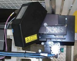
To attain the level of precision required in laser processing, wafers must first be precisely aligned. In the microDrill-EWT system, this process is performed optically using a GimaGO GO433CGigabit Ethernet camera from New Electronic Technology (NET; Finning, Germany; www.net-gmbh.com). By using an LVS TCM2 65CO/S telecentric lens, also from NET, with a collimated light source with the camera, monochromatic light is coaxially coupled into the optical axis of the lens. Since telecentric lenses provide constant image magnification as object distance varies, any perspective angle errors are reduced, increasing the accuracy of the system.
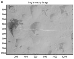
Two different procedures are used to align the wafer prior to laser processing. In the first, edge detection is performed on two different parts of one side of the wafer. By estimating a best-fit straight line between these points, the correct position of the edge is determined.
To correlate this data, a second machine-vision algorithm determines the position of wafer alignment marks that are printed on the wafer. Using this “shape model matching” procedure, the position of the wafer can be determined with sub-pixel accuracy (see figure). Both procedures ensure the precise alignment of EWT holes in the solar cell with a repeatable accuracy less than 5 μm.


