Solar Screening
C.G. Masi, Contributing Editor
Photovoltaic solar cells start out as silicon wafers a fraction of a millimeter thick. They are then trimmed to square or rectangular shape a few inches across. The manufacturer also chamfers the corners to reduce the possibility of breakage. Subsequent processing steps add several thin- and thick-film coatings that give the cells the ability to convert sunlight into electric power and channel that power to a useful load.
Working with manufacturers of solar cells, Adept Technology has been helping automate several steps in the production process. Recently, the company developed a system to automate the quality-control step between screen-printing the final set of electrodes onto cell surfaces and baking them to make permanent metallic connections.
Before baking, any flawed patterns of the conductive ink can be washed off and replaced, thus saving the wafers. After baking, such flawed wafers must be discarded, wasting the cost of the silicon material and the value added by the processing steps up to that point.
Automated inspection
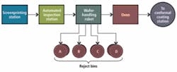
The machine-vision-based automated inspection system and the robotic wafer handler sit between the screen-printing station and bake oven on the electrode-printing production line (see Fig. 1). This is the next-to-last step in the production process, and wafers have already gone through several thin-film coating procedures to make them convert light to electricity efficiently.
null
Printing is a silk-screening process that lays down a pattern of conductive-ink electrodes. The ink consists of fine metal particles suspended in a two-part fluid consisting of a volatile solvent and an organic binder. After the screen pattern has been laid down, the solvent rapidly evaporates, leaving the metal particles held in place by the binder.
This is the stage at which it pays to inspect the pattern and recycle wafers with printing flaws. At the same time, cracks, contamination, and any other flaws in the wafers are investigated.
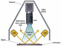
The inspection unit mounts into a light shield shaped like a truncated pyramid mounted over the conveyor line carrying wafers (see Fig. 2). The camera mounts in the upper portion, and a row of LED lights on either side of the conveyor illuminates wafers as they come by. The conveyor runs at a constant speed, with the LEDs being strobed to stop the motion.
At 26-in. high and covering a 12-in.2 footprint, the inspection unit is designed to mount 1 in. above the conveyor. This allows the light shield to exclude most ambient light while allowing wafers to move freely on the conveyor. The LED light lines are positioned so that specular reflections from the wafer surfaces miss the camera aperture and are absorbed by the light shield’s inner surface.
The system uses a Basler piA2400-12gm Gigabit Ethernet camera connected to Adept’s proprietary Smart-Vision EX vision controller. The unit is a PC-based vision controller running the company’s Automation Control Environment (ACE) and AdeptSight machine-vision software.
ACE is an integrated, point-and-click development environment with configuration tools and basic programming features for robotics applications. AdeptSight includes utilities for vision-guided and inspection applications.
The twin requirements of automated inspection and robot guidance call for different analysis algorithms applied to the same image. As the wafer moves on the conveyor, the first step is to acquire an image from the camera and upload it over the GigE connection to the vision controller for processing.
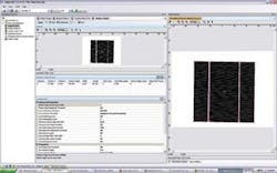
Thresholding and edge finding bring out the wafer outline as well as highlighting the screen-printed electrodes. Inspection tasks are broken into three areas: print inspection, inspection for chips, and pattern recognition. Print inspection ensures the electrode edges are crisp, form the correct pattern, and are properly registered with the wafer edges (see Fig. 3).
Inspection for chips ensures that the wafer outline does not vary from the correct size and shape: All edges must be straight; dimensions must be correct; and the corner chamfers must also be correct. Cracks appear as extraneous irregular lines that can be highlighted by enhanced contrast and thresholding. Pattern-recognition algorithms search for anything out of the ordinary such as cracks or broken ink lines. Linear measurement algorithms verify correct placement of ink patterns that are supposed to be there.
Wafer handling
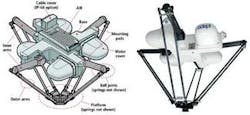
The wafer-handling station following the inspection uses an Adept Quattro robot with an unusual robotic gripper and coordinates with the vision system to automate both the inspection and handling of the wafers. The Quattro robot is a variation of the fastest type of robot available: the delta robot.
The older delta robot design has three “arms” attached to a “base” mounted over the work space. Each arm consists of an upper member—which is driven by a servomotor built into the base—and a lower member attached to a platform that carries a gripper (or whatever end effector the application calls for).
Passive joints at the lower member’s ends allow the arms to flex in a coordinated way under the influence of the separately controlled servomotors. A rod driven by a fourth servomotor rotates the gripper as needed, providing the robot with a fourth degree of freedom.
Calculating servomotor rotations to effect a required motion, however, is more complicated for a delta-robot controller than for, say, a conventional six-axis selective compliant articulated robot arm (SCARA) because the delta robot’s control degrees of freedom do not match any spatial coordinate system. To make a motion along any given axis requires coordinated action of all servomotors.
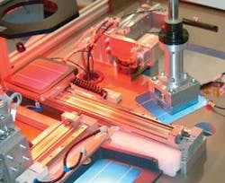
The Quattro robot differs from delta designs by having a fourth arm and no central rod. The rotational degree of freedom is made possible by providing “shoulders” in the base that move the robot’s four arms relative to each other. This arrangement makes it possible to increase the Quattro robot’s strength, speed, and agility relative to delta designs, but it also further complicates the motion controller’s kinematic calculations (see Fig. 4).
In another departure from conventional material-handling robot practice, rather than use a more traditional suction-gripper technology to pick up and move wafers, Adept’s design uses a gentler method based on Bernoulli’s principle. Suction grippers use vacuum to pull the wafer against an elastomeric cup. Friction between the cup lip and the wafer then provides the force needed to move the wafer.
Bernoulli’s principle, on the other hand, shows how to use positive air pressure to pull the wafer close to, but not in contact with, a flat plate. The principle says that along a streamline, air pressure is inversely proportional to air speed squared.
Air forced through a narrow gap between the gripper plate and wafer must move rapidly to escape. Once outside the gap, the air effectively slows to a stop. Thus air pressure in the gap must be much lower than atmospheric. Ambient pressure will press the wafer close to, but not in contact with, the plate. The wafer cannot make contact with the plate, since that would block the airflow and remove the effect.
Suction grippers create a concentrated stress around the suction inlet port, whereas the Bernoulli gripper spreads the stress over the whole gripper plate. This phenomenon greatly reduces the maximum stress level in the wafer and subsequent breakage.
Robot guidance
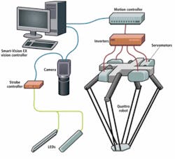
Robot guidance needs are fairly simple. The robot needs to know exactly where the wafer center is on the conveyor and what its orientation is so that it can correctly pick up any wafer that needs to be moved and avoid collisions during movement. The vision controller sends information via FireWire about part locations and motion control to a motion controller and multiaxis servomotor drive housed in the robot’s base (see Fig. 5).
Observing the angles that edges make with the image frame provides orientation information. The controller can then transform to a rotated coordinate system aligned with the wafer edges. This also helps the wafer inspection task. Finally, finding the wafer center is a matter of averaging the coordinates of opposite edges and rotating the results back to the conveyor-based coordinate system.
It would be possible to determine the conveyor speed by calculating wafer-center locations in two subsequent images, but it is better to rely on sensors built into the conveyor system. A vision-based measurement only provides one average speed measurement during a particular time interval and cannot capture slight variations in conveyor speed that might affect positioning by the time a wafer reaches the robot position. Conveyor speed sensors, on the other hand, can provide constant real-time monitoring for more accurate positioning.
For wafers that do not pass inspection, the vision controller has to decide into which of four reject bins they should go: those that can be cleaned and reprocessed, and those with different kinds of uncorrectable defects, such as corner chips, edge chips, and cracks. Since different defects arise from different causes, separating according to defect type helps continuous process improvement efforts.
features, advantage, benefits
Adept Technology found that the existing production process at a solar cell manufacturer was bogged down by reliance on manual inspection to ensure the quality of screen-printed electrodes before they were permanently baked onto silicon wafer surfaces. “With several different people looking at wafers from shift to shift,” Todd Reynolds, applications engineer at Adept, says, “one person rejects more cells that should pass, and others pass more cells that should have been rejected.
“Combining machine vision and robotics allows for less waste,” he adds. “We’re able to look for things like length and width of wafer. That allows us to get a refined center for the wafer for handling with robots. We can find chips and cracks on the wafer and inspect the printed lines for a variety of different defects.”
Improving throughput and yield near the end of the production process will have a major impact on total manufacturing cost.
Company Info
Adept Technology, Pleasanton, CA, USA
www.adept.com
Basler Vision Components, Ahrensburg, Germany
www.baslerweb.com

