Scanning the Bow
Andrew Wilson, Editor
After initially being deployed to power satellites in the 1960s, solar cells have seen deployment in a number of other areas—due to the decreasing cost of wafer production—notably remote private homes, pumping stations, and telecom network installations. With further cost decreases combined with economic subsidies, solar power has also become economically attractive for private homes and large-scale production sites. As one of the largest and fastest-growing energy sectors, the market for photovoltaic solar energy has, according to many estimates, enjoyed an average growth rate of approximately 40–60% over the last few years.
In silicon solar-cell production, either polycrystalline or monocrystalline material is generally used. Polycrystalline silicon for photovoltaic applications is produced by casting methods and monocrystalline silicon is prepared in a Czochralski growing process. After the ingots are cut to wafers, they are doped to create the photo-active p/n junction. Contacting of the photo cells is then performed by screen-printing metallic thick-film pastes onto the wafer. For the backside contact, aluminum paste is used. After the solar cells are tested, they are combined into solar modules in a continuous soldering procedure. Finally, they are packed between glass plates and retested.
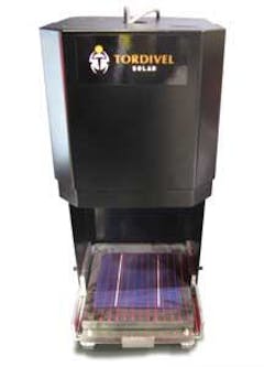
While a large number of companies are involved in the solar energy industry worldwide, only a few large companies manufacture wafers, cells, and solar panel modules. “At these companies,” says Thor Vollset, chief executive officer of Tordivel, “there is a requirement to automate and test the production quality of the wafers as they move from ingots to finished solar panels.” While vision-based inspection systems may be used to detect scratches and broken edges, others are used to determine the thickness of wafers or the sawmarks on the wafer surface. Some, such as the system developed by the newly formed Tordivel Solar—a spin-off from Tordivel—are designed to measure the bow of the wafer or the solar cell as it passes along a production line (see Fig. 1).
“Before the wafers can be combined into solar modules,” says Vollset, “they must be tested for uniformity. Because these wafers are transported through the production process on belt-driven conveyors, any non-uniformity or bowing of the 180-μm-thick wafer will cause the wafer to break further along the production line. And the breakage rate is predicted to increase as wafers are made thinner—down to 100 μm in a few years.” As a result, the production process may be stopped and excess waste generated. By measuring the bow, countermeasures to reduce bowing can be implemented.
At VISION 2008, held in Stuttgart, Germany, Tordivel showed an offline version of an automated machine-vision system designed to measure the bow of solar cell wafers. “The offline system requires an operator to manually load each individual wafer,” says Vollset. “The production version of the system will allow wafers to be automatically imaged and their uniformity measured as they pass along the production line.”
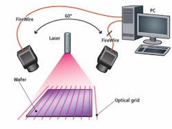
Vollset and his colleagues developed a system that employs a 3-D imaging technique to measure the uniformity of the wafer. After the wafer is placed below the system, a Lasiris laser from StockerYale projects an array of 11 fine laser lines onto the wafer. Two Flea2, 1.4-Mpixel cameras from Point Grey Research—each located 30° from the vertical axis—are used to capture two images of the projection lines (see Fig. 2). Images are then transferred to a host PC using a Fireboard800-e V.2 1349b OHCI PCI-Express FireWire adapter and the Fire-I Software 3.71 from Unibrain.
Because the angle between the projected laser light and the cameras is known, triangulation methods can be used to determine the relative height of the wafer along the laser line profiles. “Although a single laser/camera combination could be used to measure this,” says Vollset, “using two cameras results in twice the amount of data and, by comparing measurements from both cameras, an improvement accuracy of SQRT (2) or 1.415 can be achieved.” After captured images are stored in the host PC memory, relative height data is measured using Tordivel’s own Scorpion Vision 6.3 software, which features a 3-D measurement option.
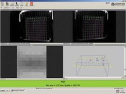
To produce a 3-D image of the wafer, 10 height points are calculated along each of the 11 laser lines in each of the two images. This results in two images with 110 height points uniformly spaced across the wafer (see Fig. 3). The results of these height points are then averaged on a pixel-by-pixel basis and the resulting data is a 3-D point cloud that provides the x and y position of the measurement across the wafer and its height (z) information. The 3-D map is also displayed on the PC monitor.
To determine the uniformity of the wafer, a blue bounding box is automatically generated to encompass all of the points in the 3-D point cloud. All of the points in this bounding box are then randomly searched to see how they best fit a plane. As the system randomly searches through the points, any 20 points that fit a plane are located or else rejected. By performing 1000 random iterations on these points, the best 10 candidates that fit a plane are stored, after which a plane consisting of the most points and least deviation from one of the selected candidates is determined.
After this process is complete, measuring the bow of the wafer is straightforward since all that is required is a calculation of the furthest point away from each side of the plane. The results of this deviation can then be displayed as a grayscale intensity map showing the gradient height of the wafer. “This map is made relative to the fitted plane,” says Vollset.
Capable of measuring one wafer per second, the Tordivel Solar system costs €25,000 and is currently undergoing trials at several major solar-panel manufacturers in Europe. According to Vollset, fully operational production-line systems will be deployed in early 2009.
Company Info
Point Grey Research
Richmond, BC, Canada
www.ptgrey.com
StockerYale, Montreal, QC, Canada
www.stockeryale.com
Tordivel, Oslo, Norway
www.scorpionvision.com
Unibrain, San Ramon, CA, USA
www.unibrain.com


